Software&Computing: Physics of nano-optics spur sophisticated models
MAXIM SUKHAREV
Even as we seek smaller and faster chips to run our computers, we are rapidly approaching fundamental limits of conventional semiconductor electronics. One possible solution is to replace electrons with photons by developing photonic circuitry. The difficulty is in efficiently controlling photons at the nanoscale.
The emerging field of plasmonics offers such a possibility by exploiting evanescent electromagnetic fields highly enhanced by surface plasmons. Plasmonics has a long history of research: A work published in 1908 by Gustav Mie may be considered as the first “plasmonics” paper underlying fundamental concepts of surface-plasmon resonance. However, it took scientists almost a century to fully make use of this phenomenon, mainly because of a lack of proper nanofabrication technology.
A metal particle exhibits strong scattering properties due to the collective excitation of conductive electrons in its surface layer (surface plasmons). It is important to note that the plasmon resonance is in the visible region for noble-metal nanoparticles, making this phenomenon very attractive for a wide variety of applications. Several other aspects unique to plasmon resonance include strong sensitivity of the resonant wavelength to the geometry of a particle, its environment, and incident polarization and phase (see Fig. 1).
Although the Mie theory provides an analytical recipe to calculate absorption and scattering, it is limited to spherical geometry only. One may extend this approach to develop iteration techniques capable of describing optics made of arrays of spheres. Other semi-analytical approaches can capture scattering by ellipsoids. Nonetheless, more complex structures usually require computationally intensive numerical solutions of Maxwell’s equations on a grid.
Modeling approaches
Many types of numerical tools exist for modeling nano-optics. For each particular problem, one has to carefully choose the best technique based on a balance between the technique’s efficiency and precision. From an applications point of view, the easiest approach to work with is a finite-difference scheme, which can be implemented in either the time domain (finite-difference time-domain, or FDTD) or the frequency domain (FDFD). The former is widely used in plasmonics due to its fairly simple programming. However, FDTD is limited by the fact that one needs to take into account material dispersion in the time domain whereas FDFD allows researchers to directly feed experimental ellipsometry data into the code. Both FDTD and FDFD have their own advantages and drawbacks.
Another fairly simple and hence widely used scheme, discrete dipole approximation (DDA), considers nanostructures as entities comprised of many pointwise dipoles with a given dipole moment. Because electromagnetic fields for a single Hertzian dipole can be expressed analytically, DDA exploits the linearity of Maxwell’s equations, adding fields generated by each dipole together. Despite many attractive features, this technique has a serious disadvantage due to the divergence of the electromagnetic field at the grid point, where the dipole is located.
Probably the most advanced method for simulations of optical properties of nanomaterials is based on the finite-element method (FEM). Unlike finite-difference schemes, it discretizes the simulation domain using special nonuniform and nonrectangular meshes. The finite-element method is less common in plasmonics due to its programming complexity and difficult parallel implementations. However, it offers very precise description of almost any geometry.
Many commercial packages are based on these techniques. Probably the most reliable software based on FDTD with a strong emphasis on nano-optics is distributed by Lumerical Solutions (Vancouver, BC, Canada). It provides a simple graphical user interface requiring a next-to-nothing knowledge of numerics. A rich database of various materials makes Lumerical FDTD attractive for researchers. Recently it began to offer parallel implementation, allowing users to run their codes on local multiprocessor machines, significantly reducing execution times for simulations.
Several commercial products provide a graphical user interface similar to the Lumerical FDTD but based on FEM techniques. Perhaps the most prominent is the software package by COMSOL (Burlington, MA), which offers integration with the MATLAB package and parallel implementation of simulations.
Custom software
Despite the wide variety of commercial products, researchers often need capabilities that reach far beyond those of black-box commercial codes—for example, integrating numerical solutions of Maxwell’s equations on a grid with additional simulations, which are not usually included in commercial packages.
As a first example, we consider recent applications of optimal design of plasmonic devices. The optical properties of metal-nanoparticle arrays depend sensitively on various parameters that include the shapes of the particles, their relative arrangement, and the polarization of the incident field. Advances in nanofabrication methods allow experimenters to control the nanostructure-fabrication process to an outstanding degree of precision. This calls for the development of a systematic design tool that can be used to optimize the geometry of nanoconstructs to design optical materials with specific desired functionalities. The latter can be accomplished by blending together numerical integration of Maxwell’s equations with an evolutionary algorithm such as genetic-algorithm optimization.
Genetic algorithms belong to the class of search techniques inspired by the biological process of evolution by natural selection, and can be used to construct numerical-optimization techniques that perform robustly on problems characterized by ill-behaved search spaces where standard algorithms, such as gradient-search methods, would typically halt near a local extreme. The stochastic nature of the genetic algorithm makes it a numerically stable functional optimizer. One of the great advantages of the genetic algorithm is that no numerical derivatives of the fitness function with respect to the model parameters need be computed. However, as in most stochastic solutions, a large number of evaluations are necessary in order to find a global extreme. If the evaluation is computationally expensive, the forward-modeling approach can become impractical.
One can consider a general nanoconstruct in which, for example, transmission of electromagnetic energy depends on a set of adjustable parameters such as incident-field parameters (laser-pulse duration, wavelength, polarization, form of time-envelope function, and so on) and material parameters (geometry of an array of metal nanoparticles). The fitness function in genetic-algorithm optimizations is in our case an observable that is, for instance, averaged over time—such as electromagnetic energy detected by a near-field detector or a preferred electromagnetic field distribution.
Where quantum and classical physics meet
Pushing optical devices to the nanoscale limits requires a great deal of understanding of processes that lie at the intersection of quantum mechanics and classical physics. Recently developed plasmonic optical detectors, for instance, operate at a single-molecule level. To fully understand the physics of interaction of electromagnetic radiation with quantum objects coupled to materials such as metal nanoparticles, one needs to be able to properly simulate dynamics governed by Maxwell’s equations and the Liouville equation. The latter is necessary to scrutinize the quantum dynamics of atoms or molecules driven by local electromagnetic fields.
It is impossible to carry out such simulations using commercial software, because the simulations require direct access to the core of a Maxwell’s equations integrator. Hence one has to be able to either create custom code or rely on open-source software.
As an example of such simulations, we consider the general problem of interaction of strong laser pulses with an array of L-shaped silver nanoparticles embedded in resonant quantum media. It has been recently shown that arrays of nanoparticles with no center-of-inversion symmetry exhibit birefringence, modifying the polarization of incident radiation. In particular, L-shaped nanoparticles have two well-defined surface-plasmon resonances associated with the axes of symmetry. If the polarization of a pump pulse does not lie along one of these axes, the total electromagnetic field becomes elliptically polarized.
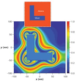
An example illustrates the spatial distribution of the atomic ground state population of a quantum medium after pumping the system with a 40 fs laser pulse (see Fig. 2). Clearly, this distribution is significantly inhomogeneous, exhibiting interesting ripples associated with high electromagnetic-field gradients near the nanoparticle. Similarly, populations of the excited atomic states are also strongly inhomogeneous and depend on the polarization of the pump pulse. Further simulations that include a low-intensity probe pulse demonstrate that the pump drastically modifies the macroscopic refractive index of the system. Moreover, the modified refractive index is appreciably anisotropic.These results suggest an exciting new research direction in plasmonics, in which both the geometry of metal nanostructures and the presence of pump pulses govern the refractive index of a system. One can apply optimization techniques such as genetic algorithms, for instance, to design materials with desired optical properties. It should be noted that the modified refractive index is highly dynamical and does depend on many parameters such as lifetime of the excited atomic states, dephasing, and others.
REFERENCES
1. T.W. Ebbesen et al., “Surface plasmon circuitry,” Physics Today, 61, 44 (2008).
2. W.A. Murray and W.L. Barnes, I, 19, 3771 (2007).
3. M. Sukharev and T. Seideman, J. Phys. B: At. Mol. Opt. Phys., 40, S283 (2007).
4. J. Yelk et al., J. Chem. Phys., 129, 064706 (2008).
Maxim Sukharev is assistant professor at the Department of Applied Sciences and Mathematics, Arizona State University, Mesa, AZ 85212; e-mail: [email protected].

