NOVEL DISPLAYS/IMAGERS: Compressive sensing architecture advances infrared camera design
RICHARD G. BARANIUK, KEVIN F. KELLY, SANJAY KRISHNA, and ROBERT F. BRIDGE
New detector materials such as superlattices, quantum dots, carbon nanotubes, and graphene can significantly enhance the performance of infrared (IR) cameras by reducing detector noise, increasing sensitivity, and/or decreasing detector cooling requirements. However, a long development cycle is typically needed to produce megapixel-count focal-plane arrays (FPAs) using new detector materials. Compressive sensing (CS) technology allows new detector materials to be incorporated early in their life cycle because CS cameras use a single-pixel detector and do not require a high-pixel-count FPA.
IR detector technology
At wavelengths beyond one micron, IR cameras cannot use commodity complementary metal-oxide semiconductor (CMOS) material to build FPAs as this material is insensitive to these longer wavelengths. For non-CMOS detector materials, the materials science lags decades behind that of CMOS, making IR cameras expensive. The detector materials used in IR cameras have various limitations such as high cost and high dark noise, and significant research is ongoing to develop new materials that overcome these limitations.
High-performance IR detectors are currently dominated by bulk indium antimonide (InSb) in the midwave IR (MWIR) region (3–5 µm) and mercury cadmium telluride (MCT) in the longwave IR (LWIR) region (9–12 µm). Both these semiconductors have bandgaps in the appropriate bands; incident photons that are above the bandgap create photogenerated carriers (electrons in the conduction band and holes in the valence band)—usually, in a biased p-n junction. Such interband devices, with an in-built field, are referred to as photovoltaic detectors. These high-performance detectors need to be cooled to reduce the dark current associated with thermal processes.
Emerging IR detectors
Intersubband devices based on transitions in quantum wells and referred to as quantum-well IR photodetectors (QWIPs) are promising for the LWIR regime. Most present-day QWIPs are operated in a photoconductive mode where an external bias is applied to tilt the energy bands and collect carriers that are generated when incident photons are absorbed due to the resonance in the intersubband states. However, the QWIPs are plagued with large dark current and low quantum efficiency due to the nature of the intersubband transitions. Several solutions including corrugated QWIPs, low-noise QWIPs, and enhanced QWIPs (E-QWIPs) have been developed to improve performance.
In the past decade, there has also been active interest in IR detectors based on intersubband transitions in quantum dots. These quantum-dot IR photodetectors (QDIPs) are expected to have a lower dark current thanks to their three-dimensional (3D) confinement and increased lifetime due to reduced scattering processes. More recently, quantum-dots-in-a-well (DWELL) detectors have been proposed that combine the advantages of QWIPs (such as control over the operating wavelength) with the advantages of QDIPs (such as normal incidence operation, increased lifetime, and 3D confinement).1 And a very promising technology based on miniband transitions in Type II strained layer superlattices (T2SL) of the indium-arsenide/indium-gallium-antimonide (InAs/InGaSb) material system have emerged.2 They have large quantum efficiency and are based on III-V semiconductor technology. However, the surface passivation schemes of side walls in this system must be carefully considered before demonstrating high-performance FPAs.
Compressive sensing changes the rules
High-resolution compressive sensing (CS) cameras can use just a few- or even a single-pixel detector. Because they do not require a high-pixel-count FPA, alternative detector materials can be incorporated years earlier than in an FPA design.3
The CS architecture captures compressed data as the image is being taken, not after the fact. In a conventional camera, the large amount of raw data acquired often necessitates immediate compression in order to store or transmit that data. This process has two major potential drawbacks. First, acquiring large amounts of raw image data (a large number of pixels N) can be expensive—particularly at IR wavelengths where CMOS detector technology is ineffective. Second, compressing raw data can be computationally demanding. Fortunately, CS provides a way around these drawbacks. A CS camera directly acquires random projections without first collecting the N pixel values and can obtain an image with a single-detection element while measuring the image far fewer times than the number of pixels. This means CS is significantly faster than a Nyquist raster scan, and in many instances, can produce a higher-resolution image than an FPA.
The CS camera is based upon a fundamental concept of signal processing; namely, that images typically contain structure that enables parsimonious representation. High-performance image compression algorithms take advantage of this structure through a decorrelating transform that compacts the correlated signal’s energy into a smaller number of essential coefficients. These transform coders take advantage of the fact that many signals have a sparse representation in some basis [the discrete cosine (JPEG) or wavelet transform (JPEG2000)], meaning that just K << N of the N transform coefficients are significant and need to be stored or transmitted. If an image is JPEG or JPEG2000 compressible, then CS can be used to efficiently acquire it.
Standard image acquisition and compression works as follows: (i) acquire the full N-sample image x; (ii) compute the complete set {θ(n)} of transform coefficients θn = <ψn, x>; (iii) locate the K largest coefficients and discard the (many) small coefficients; and (iv) encode the values and locations of the largest coefficients. In cases where N is large and K is small, this procedure can be quite inefficient; much of the output of the analog-to-digital conversion process ends up being discarded, although it is not known a priori which pieces are needed.
For a given image, it is possible to directly estimate the set of large coefficients that will not be discarded by the transform coder. The theory of CS demonstrates that a signal that is K-sparse in one basis (call it the sparsity basis) can be recovered from M = cKlog(N/K) nonadaptive linear projections onto a second basis (call it the measurement basis) that is incoherent with the first, where c is a small constant (typically around 2). Amazingly, a random measurement basis is incoherent with all fixed sparsity bases. Recovery is typically performed by a sparsity-inducing linear program or greedy algorithm.4
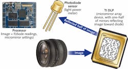
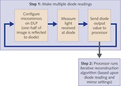
A CS camera architecture incorporates a microcontrolled mirror array configured using a measurement basis and a single-pixel detector. This hardware optically computes incoherent image measurements as dictated by the CS theory; CS reconstruction algorithms are then applied to obtain the acquired images. A CS system directly acquires a reduced set of M incoherent projections of an N-pixel image x without first acquiring the N pixel values. The camera is “progressive,” meaning that better quality images (larger K) can be obtained by taking more measurements M.
Building a CS camera
In a CS camera, the incoming image is focused upon a Texas Instruments (Dallas, TX) digital-light processing (DLP) micromirror device (see Fig. 1). Each of the N micromirrors corresponds to an image pixel. For the randomized basis, we select random vectors containing only the values 0 and 1. Thus, each measurement consists of the sum of a random selection of about one-half of the pixels of an N pixel representation of the image. The detector acts as a photon “bucket,” or light meter, and measures the total light in the randomly selected pixels. Then, M measurements are obtained by repeating this process M times, each time with a different random selection of pixels.A practical and interesting attribute of CS is that one-half of the total light of the entire image reaches the single detector, increasing the sensitivity of the measurement process over megapixel FPAs wherein each pixel receives on average just one-millionth of the total available image light. Also, if a CS camera needs to communicate its compressed data over a communication link, the data is naturally encrypted since the diode readings are meaningless unless one also knows each associated mirror pattern.
In addition to the advantages of reduced sensor cost, reduced data volume, and enhanced sensitivity, the CS camera’s single-pixel design also allows the incorporation of new detector materials into high-resolution cameras before they are able to be manufactured into high-pixel-count FPAs. To modify an existing CS camera to use new a new detector material, one simply replaces the diode and its associated analog-to-digital converter, dramatically reducing time to market and production costs. All other elements of the camera can remain the same.
REFERENCES
1. A.V. Barve et al., “Review of current progress in quantum dot infrared photodetectors,” Laser & Photon. Rev., 1–13 (2009).
2. A. Rogalski and P. Martyniuk, Infrared Phys. Technol., 48, 1, 39–52 (2006).
3. M.F. Duarte et al., “Single-Pixel Imaging via Compressive Sampling,” IEEE Signal Processing Magazine, 25, 3, 83–91 (March 2008).
4. R.G. Baraniuk, “Compressive Sensing” Lecture Notes, IEEE Signal Processing Magazine 24, 4, 118–120 (July 2007).
Richard G. Baraniuk is a professor and Kevin F. Kelly is an assistant professor at Rice University, P.O. Box 1892, Houston, TX 77251-1892. Sanjay Krishna is a professor at the University of New Mexico, 1313 Goddard St. SE, Albuquerque, NM 87106. Robert F. Bridge is CEO of InView Technology Corp., 2110 Whitehorse Trail, Suite G, Austin, TX 78757; e-mail: [email protected]; www.inviewcorp.com.


