PHOTONIC CRYSTALS: Photonic crystals approach visible-light functionality
SAULIUS JUODKAZIS and SAJEEV JOHN
Evolution has sensitized the human eye to green light at wavelengths around 530 nm. Creation of structures and devices that can control and handle light propagation, detection, and emission at the visible spectral range will always be of the utmost importance due to their ability to directly interface with our sense of vision. Moreover, the forms of solar energy storage—whether hydrocarbon fuels, food generated via photosynthesis, or renewable energy resources such as wind and direct light—are all dependent on the spectral window through which Earth is receiving energy from the Sun. The major part of this energy reaches us in the visible spectral range and underpins our lives; essentially, light-matter interaction at visible wavelengths holds answers to our future food and energy needs.
Photonic crystals (PCs) are powerful light handlers and are used in numerous ways to control light on a sub-wavelength scale, including the ability to completely trap or localize light, to guide it in three-dimensional (3D) circuit paths on a microchip without scattering or diffraction loss, and to realize unprecedented forms of strong coupling between light and matter.1,2 However, due to fabrication challenges, the PC functionality window in the past has stopped short of entering the visible spectral range.
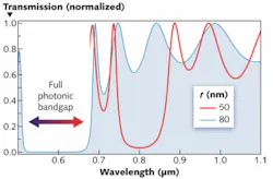
The largest technological challenge to fabrication of visible-light PCs is to structure materials in all three dimensions with spatial period smaller than typically half of the light’s wavelength so that PCs will have a transmission block—an omnidirectional photonic bandgap (PBG). In the spectral range of the PBG no light propagates in the crystal in any direction due to complete destructive wave interference. If a defect is placed in the otherwise periodic dielectric microstructure of the PC, it acts as a trapping center to which light can be localized. The confinement volume of the trapped light can be much less than a cubic wavelength and lifetime of the captured light is limited only by intrinsic absorption in the underlying material.
Sub-100 nm structuring challenges
Nature’s approach to nanostructuring is via self-organization and structural encoding of nanoscale architectures at the DNA level. The physical structure of a butterfly wing and the subtle balance between order and disorder in the structure is responsible for the structural color (see Fig. 1).3 Interestingly, the color appearance is omnidirectional in a wide range of incidence angles due to the presence of disorder. However, naturally occurring materials and systems do not scatter light strongly enough to create a PBG or to trap light. This requires nanolithography using materials with a high refractive index greater than two. Modern top-down approaches of nanofabrication have only recently entered true nanoscale structuring where the feature sizes in all dimensions can be made at sub-100 nm levels. One promising example of such technology is the focused ion beam, which can create high-aspect-ratio 3D structures by removal of dielectric host material in arbitrary fashion by a direct-write approach.
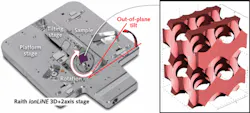
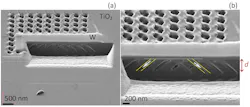
Even though the fabrication of PCs with visible-light PBGs by 3D sculpturing using ion beams is challenging, our group used a 3D ion beam lithography (IBL) approach to fabricate a 3D PC slanted-pore (SP) structure with a wide and robust PBG by a simple two-step, direct-write processing of rutile crystalline titanium oxide (TiO2). The geometry of the unit cell is chosen for the PBG at visible wavelengths around 633 nm. The fabrication technique, using a Raith GmbH (Dortmund, Germany) ionLINE setup, does not require time- and material-consuming steps of resist and mask coatings with subsequent wet or dry processing. Instead, a direct-patterning approach by gallium (Ga) ions is used to sculpture 3D structures out of the crystal with tens-of-nanometers resolution. The capability of direct write at arbitrary angles in 3D mode is a distinctive feature of 3D IBL.Despite challenges, further improvements in 3D IBL sculpturing are in reach. Optimization of milling can produce larger pores and patterning larger areas will enable detailed optical characterization. Namely, by introducing trepanning and concentric outward scanning of strongly focused ion beams during milling, together with optimization of the chemical doses and other enhancements, PCs functional at visible wavelengths can be fabricated. It is noteworthy that the other popular methods used in materials structuring at the sub-micrometer range such as direct laser writing in photopolymers (a serial and parallel methods) and dry plasma etching (parallel) cannot easily be adopted for sub-100 nm nanofabrication.7,8 The 3D IBL approach is promising for practical applications especially because it is a maskless and direct-write process.
Photonic crystals have important practical applications in confining light on an optical microchip for all-optical information processing, in trapping and absorbing light in thin films for efficient solar energy harvesting, as novel light emitters, as optical sensors, and for photocatalysis, to mention only a few.9,10
ACKNOWLEDGMENTS
This work has been partly supported via the Joint Development Program (JDP) between Raith GmbH, Swinburne University of Technology, and the Natural Sciences and Engineering Research Council of Canada (Ottawa, ON, Canada). Saulius Juodkazis is grateful to the Australian Trade Commission (Austrade) for supporting research visits to Raith GmbH.
REFERENCES
1. S. John, Phys. Rev. Lett., 58, 2486–2489 (1987).
2. E. Yablonovitch, Phys. Rev. Lett., 58, 2059–2062 (1987).
3. A. Saito et al., J. Nanosci. Nanotechnol., 11, 2785–2792 (2011).
4. O. Toader and S. John, Phys. Rev. E, 71, 036605 (2005).
5. S. Juodkazis et al., Opt. Exp., 19, 7, 5802–5810 (2011).
6. A. Chutinan and S. John, Phys. Rev. A, 78, 2, 023825 (2008).
7. S. Juodkazis et al., J. Appl. Phys., 106, 051101 (2009).
8. S. Takahashi et al., Nat. Mater., 8, 721–725 (2009).
9. A. Chutinan, S. John, and O. Toader, Phys. Rev. Lett., 90, 12, 123901 (2003).
10. S. John and R.Z. Wang, Phys. Rev. A, 78, 4, 043809 (2008).
Saulius Juodkazis is a professor in the Faculty of Engineering and Industrial Sciences at the Centre for Micro-Photonics, Swinburne University of Technology, Hawthorn, VIC, 3122 Australia; e-mail: [email protected]; www.swinburne.edu.au. Sajeev John is a professor in the Department of Physics, University of Toronto, Toronto, ON, m5S 1A7 Canada; e-mail: [email protected]; www.utoronto.ca.
![FIGURE 1. Nanotechnology can reproduce nature’s highly reflective structures [3]; that is, the wing structure of a Morpho blue butterfly (Morpho didius) shows an omnidirectional color, unlike a reflection from a grating structure. FIGURE 1. Nanotechnology can reproduce nature’s highly reflective structures [3]; that is, the wing structure of a Morpho blue butterfly (Morpho didius) shows an omnidirectional color, unlike a reflection from a grating structure.](https://base.imgix.net/files/base/ebm/lfw/image/2016/01/pennwell.web.450.169.png?auto=format,compress&fit=fill&fill=blur&q=45?w=250&width=250)


