SPECTROMETERS: Microspectrophotometers take a closer look

The microspectrophotometer is a hybrid instrument that integrates the magnifying power of a microscope with a spectrophotometer. These microspectroscopy instruments are used to measure molecular spectra of microscopic samples, or microscopic features of large-scale samples, from the deep ultraviolet (UV) to the near infrared (NIR). Depending upon the configuration, the microspectrophotometer can measure absorbance, reflectance, and the emission spectra—such as fluorescence—of sub-micron-sized sample areas. With the addition of specialized algorithms, the microspectrophotometer can also measure the thickness of thin films or act as a colorimeter for microscopic samples.
The advantages of such tools are numerous. The most obvious advantage is that spectra can be acquired from microscopic sample areas; these instruments can measure sub-micron features and therefore require very small amounts of sample in either solid or liquid form, with little or no sample preparation. Or they can be used to map the spectral characteristics of samples with very high spatial resolution. Color comparisons by microspectroscopy are typically more accurate than with the naked eye as microspectrophotometers can analyze the spectra from 200–2200 nm (well beyond the range of the human eye), correct for lighting variations, and measure the intensity of each wavelength of light. The microspectrophotometer is also designed to yield the highest-quality spectroscopic data from the smallest samples, with none of the drawbacks found with adapter modules for macroscale spectrophotometers. Flexibility is another key feature: A UV-visible-NIR (UV-VIS-NIR) microspectrophotometer is able to acquire images and spectra by absorbance, reflectance, fluorescence, and other types of luminescence—all with the same instrument.
Before the advent of microspectroscopy, the only way to analyze many types of microscopic samples was to use microchemical testing and then some sort of visual examination. Unfortunately, these processes destroy a sample, require large amounts of a sample, and suffer from the inaccuracies of the human visual system. But UV-VIS-NIR microspectrophotometers can analyze microscopic samples without destruction and can detect sample variations that would not be apparent by eye. Speed is another issue: Microchemical tests can take anywhere from minutes to days to complete. A microspectrophotometer can measure a spectrum in milliseconds.
Anatomy of a microspectrophotometer
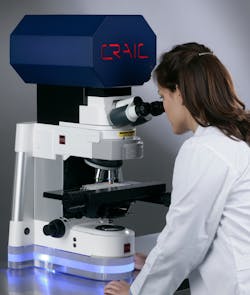
The modern microspectrophotometer integrates a highly sensitive spectrophotometer with a microscope optimized for spectroscopy and imaging (see Fig. 1). The microscope must have an operational spectral range from the deep-UV to the NIR while maintaining good image and spectral quality. Standard microscopes cannot be used as they only cover a portion of the visible spectrum due to their optical designs and light sources. Instead, a customized microscope consists of air-mounted lenses of fused silica and other materials, as well as UV-enhanced mirrors, mounted in a configuration designed to evenly illuminate a sample while producing a sharp image in all regions of the designated spectral range of the instrument. Illumination is provided either with modified xenon lamps, lasers, or by mixing the output of a deuterium lamp with that of a halogen lamp. The UV-VIS-NIR microscope will also operate in a manner similar to that of a standard compound microscope, meaning that the learning curve for such instruments is shorter and the user can easily transition between different types of spectroscopic and imaging experimental setups.
The spectrophotometer itself must also be designed for microspectroscopy in order to obtain good spectral results. It must have a high dynamic range as users commonly switch from transmission or reflectance spectroscopy to fluorescence spectroscopy when measuring the same sample in order to obtain different types of spectra from exactly the same location. This operation requires the spectrophotometer to be sensitive while still maintaining an acceptable spectral resolution. Stability is also an issue as the microspectrophotometer is a single-beam instrument and reference spectra must be obtained prior to measuring a sample. The heart of the system is a high-quality array detector with thermoelectric cooling. The optical design of the monochromator is also optimized to maximize light throughput while maintaining a spectral resolution acceptable to the customer.
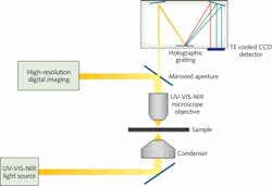
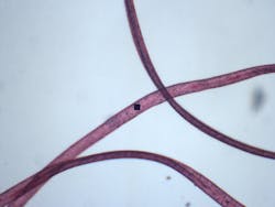
How the spectrophotometer is integrated with the microscope is probably the most important factor, however (see Fig. 2). Such features as calibrated variable apertures allow for different sampling areas and an increase in energy throughput while maintaining spectral resolution and experimental reproducibility.The job of the microscope component is to illuminate the sample and funnel the electromagnetic energy collected from the sample into the spectrophotometer. In order to do this, the user must be able to visualize the sample measurement area as well as see the surrounding sample. This means that the entrance aperture of the spectrophotometer is at the same focal plane as the sample image; a video image of the two fields shows the aperture in sharp focus over the sample in addition to the surrounding field of view (see Fig. 3). During operation, the sample stage is moved until the image of the entrance aperture is over the area of the sample to be measured. Once the aperture is aligned with the sample area of interest, the spectrum is then measured. Of course, images of the measured sample with the aperture in place can also be stored. For many research applications, this sample-aperture alignment operation is done manually. For industrial operations, this procedure is often automated.
Depending on the type of experiment to be performed, the microscope can be configured with different illumination schemes. White light allows for reflectance microspectroscopy from the deep UV to the NIR, and incident illumination can be used for fluorescence or phosphorescence microspectroscopy by using a series of filters or a monochromator with a white light source or one of a series of lasers that may be mounted to the frame of the microspectrophotometer. Transmission microspectroscopy is done with a white light focused onto the sample through the microscope’s condenser.
Compared to most modern microscopes with a limited spectral range of only 450–700 nm, the microspectrophotometer microscope spans 200–2200 nm.
From forensics to film thickness to SPR
A host of different applications have emerged since the first microspectrophotometer was built in the 1940s. With the ability to acquire spectra of microscopic sample areas, microspectrophotometers are used everywhere from university laboratories to production lines for quality control and failure analysis.
The first two major applications for microspectrophotometers in the early 1980s were analysis and small-spot thin-film thickness measurements. Microspectrophotometers are used in the forensic sciences to analyze the absorbance and fluorescence spectra of textile fibers, dyed hairs, paint chips, and even colored glass fragments. They are also used to measure the reflectance and fluorescence spectra of documents, analyzing ink and paper compositions and handwriting details nondestructively and in just a few minutes.
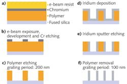
Microspectrophotometers are also built to measure the thickness of thin films used in the semiconductor manufacturing of integrated circuits. The microspectrophotometer takes either reflectance- or transmission-spectra measurements, depending upon whether the small area of the substrate to be sampled is transparent or not. Similar to the color changes seen with oil on water, these same interference patterns can be measured spectroscopically. Special software is then used to calculate the thickness of each of the films deposited on the substrate. While still an important part of quality control testing in the semiconductor industry, small-spot film thickness measurements are now used in the development and manufacture of optics, flat-panel displays, and many other devices.Materials science is advancing based on the ability of microspectrophotometers to measure transmission, reflectance, and emission spectra with a single instrument. One rapidly developing application concerns the surface plasmon resonance (SPR) effect. Surface plasmons are excited by illuminating a planar metallic surface or nanoscale metallic particles with light (see Fig. 4). Changes in the optical characteristics of these materials occur when these nanoparticles or surfaces interact with other materials. Microspectrophotometers can acquire the reflectance and emission spectra of small aggregates of nanoparticles, indicating how the spectra of the SPR material changes as the test conditions are varied. This gives the researcher the ability to “tune” that material to create specific optical effects.
Paul Martin | President, CRAIC Technologies
Paul Martin is president of CRAIC Technologies (San Dimas, CA).


