PLASMONIC LIGHT DETECTORS: Optical nano-antennae boost speed and efficiency of single-photon detectors

XIAOLONG HU and KARL K. BERGGREN
Many applications in communications and quantum optics need fast and efficient single-photon detectors. Superconducting-nanowire single-photon detectors (SNSPDs, also referred to as SSPDs) are an emerging technology for fast and efficient single-photon detection. A typical device is composed of a 4-nm-thick, 70–100-nm-wide, several-hundred-microns-long niobium nitride (NbN) wire wound in a meander structure. To operate the detector, the nanowire is cooled below 4K and biased close to its critical current. One absorbed incident visible or infrared (IR) photon can quench its superconductivity and generate a voltage pulse. Then, the absorbed energy is dissipated as thermal energy and superconductivity is restored. The nanowire is ready to detect a second photon, and the detector is therefore running in a free-running mode.
Researchers have been continuously improving the performance of the technology since it was invented in 2001.1 In particular, a 57% device efficiency was demonstrated by integrating the detector with a top reflector and an antireflection coating on the back of the substrate.2 But that detector was only 3 × 3 µm in size, too small to permit efficient light coupling.
Later, researchers fabricated a large-area detector with 30% device efficiency and put four small detectors together to cover an area sufficient for light coupling.3-5 More than 20% system-detection efficiency was demonstrated in fiber-coupled, close-cycled cryocooler systems. Another significant advance was the demonstration of photo-number-resolving capability by using multiple nanowires either biased individually4 or connected in parallel.6
However, a tradeoff exists between speed and efficiency of an individual SNSPD because on the one hand, the speed is limited by the kinetic inductance, which is proportional to the length of the nanowire, so shorter wires result in faster device reset; while on the other hand, a longer nanowire is desirable for good system detection efficiency because the nanowire needs to cover an area large enough to permit photon coupling.7 For this reason, past demonstrations of high system-detection efficiency sacrificed speed. A simultaneously fast and efficient SNSPD had remained a technological challenge.
Optical “funneling,” interference, and surface scattering
The speed/efficiency tradeoff has been dramatically improved by integrating the nanowire with metallic optical nano-antennae.8,9 We have used a short nanowire to form a sparse meander and added gold structure in the gaps and on top of the nanowire. This gold structure can behave as an optical nano-antenna to collect and “focus” the light to the NbN nanowire and thus enhance the optical absorption and detection efficiency.
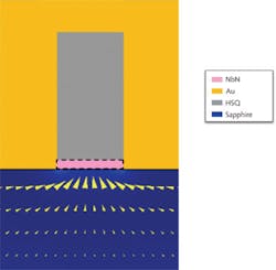
The nano-antenna effect can be heuristically explained as a combination of three optical effects. The first effect is the optical funneling by the gold-hydrogen silsesquioxane (HSQ)-gold structure, which enhances the transmission of transverse-magnetic (TM)-polarized incident photons and reflects transverse-electric-(TE-) polarized photons. This optical funneling is nonresonant (see Fig. 1). In the deep subwavelength regime, such a structure behaves as a wire-grid polarizer. Once a majority of TM-polarized incident photons are funneled into the gold-HSQ-gold waveguide, the second effect plays a role: The gold on top of HSQ serves as a reflector to reflect the funneled light. Optical interference between incident and reflected light creates an optical anti-node at the location of the NbN nanowire, maximizing its absorption. Finally, the interface between the sapphire substrate and the nanostructured gold scatters the incident light; the scattering adds additional absorption enhancement for the NbN nanowire.
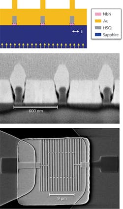
A careful design predicts that a device with a 600-nm-pitch meander covering a 9 × 9-µm active area can achieve 47% absorptance. The total length of the nanowire is 135 µm, as opposed to 371 µm in an old design covering a similar active area.
To integrate optical nano-antennae, we performed 30 kV electron-beam writing on 300-nm-thick HSQ to pattern NbN. The rest of the HSQ after etching served as the fencelike structure. Gold was evaporated and self-aligned with the HSQ structure; prior to gold evaporation, 6 nm of silicon dioxide (SiO2) was evaporated to electrically insulate the gold from the NbN nanowire and 3 nm of titanium to promote adhesion between gold and SiO2 (see Fig. 2).With optical-antenna integration, the detectors became faster and more efficient. We obtained 47±5% and 3.5±0.4% device efficiency for TM- and TE-polarizations, respectively, on this 9 × 9-µm device. The polarization sensitivity is a key feature of the antenna effect. The kinetic inductance was measured to be 100 nH; correspondingly, the reset time was calculated to be 5 ns. In order to compare this detector with other detectors, we defined a figure of merit as (active area × device efficiency/reset time). This figure of merit has been enhanced by a factor of 4.5 by the optical nano-antennae, compared to the SNSPD with cavity integration.
The enhancement effect and polarization sensitivity were observed on several devices; however, the enhancement factors varied in a large range and the device yield was low. Improving the robustness of the fabrication process is the next step after this initial demonstration.
Other applications of optical nano-antennae
Optical nano-antennae and metallic nano-structures can not only boost the speed and efficiency of SNSPDs, but can also enhance the performance of various other optoelectronic components and add additional functionalities. For example, a bow-tie antenna has been integrated with a laser diode to confine light on the nanoscale10, and a dipole antenna has been used to enhance the photocurrent of a germanium photodetector.11 More interesting physics are still being discovered and applications being developed.
ACKNOWLEDGMENT
This work was sponsored by IARPA, the National Science Foundation under NSF award No. ECCS-0823778, and the Centre for Excitonics, an Energy Frontier Research Center funded by the US Department of Energy, Office of Science, Office of Basic Energy Sciences.
REFERENCES
1. G.N. Gol’tsman et al., Appl. Phys. Lett., 79, 705 (2001).
2. K.M. Rosfjord et al., Opt. Exp., 14, 527 (2006).
3. X. Hu et al., Opt. Lett., 34, 3607 (2009).
4. E.A. Dauler et al., J. Modern Opt., 56, 364 (2008).
5. S. Miki et al., Opt. Exp., 17, 23557 (2009).
6. A. Divochiy et al., Nat. Photon., 2, 302 (2008).
7. A.J. Kerman et al., Appl. Phys. Lett., 88, 111116 (2006).
8. X. Hu et al., IEEE Trans. on Appl. Superconductivity, 19, 336 (2009).
9. X. Hu et al., Opt. Exp., 19, 17 (2011).
10. E. Cubukcu et al., Appl. Phys. Lett., 89, 093120 (2006).
11. L. Tang et al., Nat. Photon., 2, 226 (2008).
Xiaolong Hu obtained his PhD from the Department of Electrical Engineering and Computer Science at the Massachusetts Institute of Technology and is currently working as a postdoctoral research fellow in the University of Michigan, Room 2223 EECS, 1301 Beal Avenue, Ann Arbor, MI 48019; e-mail: [email protected]. Karl K. Berggren is an associate professor in the Department of Electrical Engineering and Computer Science at the Massachusetts Institute of Technology, 77 Massachusetts Ave. 36-219, Cambridge, MA 02139; e-mail: [email protected].
