OPTICS FABRICATION: High-performance mirrors excel for intracavity applications
High-performance mirrored optics are an enabling technology in a variety of high-sensitivity measurement techniques such as cavity-based absorption spectroscopy, optical atomic-clock spectroscopy, ring-laser gyroscopes (RLGs), and gravitational-wave detection. In each technique, high-reflectivity, low-loss mirrors that can operate under a variety of environmental conditions without any sacrifice in spectral performance are critical. Here, we describe how mirrors manufactured by ion beam sputtering (IBS) and using dielectric materials are designed to achieve extremely high reflectivity (R) greater than 99.99% and low loss over a broad spectral range. Particular emphasis is given to how the losses associated with light absorption, scattering, and transmission are minimized and quantified by direct measurement. An example of the importance of these mirrors in cavity ring-down spectroscopy (CRDS) will also be discussed.
Most mirrors are made using thin metal films deposited on glass and are suitable for many applications where some level of loss is acceptable. The main advantage of metals such as silver, gold, and aluminum is that they can provide R >95% over a spectral range spanning several microns. However, enhancement of the reflectivity of metal mirrors requires additional processing steps involving dielectric overcoat layers.
Despite the fact that metallic mirrors are relatively low in cost and can have a relatively high mirror reflectivity over a very broad wavelength range, they are not well suited to applications where high sensitivity and high-precision measurements demand light loss in the part-per-million range and thus require mirrors having extremely high reflectivity. An additional disadvantage of metal coatings is that they are both chemically (silver) and mechanically (aluminum, silver, gold) unstable, and in most cases it is necessary to apply a protective layer, such as silicon oxide over aluminum, to limit mirror degradation. Therefore, to overcome the inherent inadequacies associated with metal coatings, an alternative is required. One approach is to use ion-beam sputtering (IBS) to manufacture high-reflectivity, low-loss mirrors suitable for high-sensitivity laser-based instrumentation.
A dielectric mirror is formed by depositing a stack of alternating high- and low-refractive index layers on an underlying (glass, crystal, or metal) substrate. Through a judicious choice of the multilayer design, coating materials, and deposition process, it is possible to manufacture dielectric mirrors having extremely high reflectivity over a reasonably wide range of wavelengths in the ultraviolet (UV) to near-infrared (NIR) spectral region.
The key requirements when designing hard-coated, low-loss dielectric mirrors are: high (R >99.95%) reflectivity over the mirror bandwidth; operation over a range of angle-of-incidence (AOI) values for both s- and p-polarized light; and a high laser-induced-damage threshold (LIDT; for example, a LIDT >20 J/cm2 for 10 ns, 1064 nm pulses). Reflectance data for two examples of high-reflectivity dielectric mirrors designed to operate in the visible and NIR are shown in Fig. 1. In what follows we describe the performance characteristics of hard-coated dielectric mirrors, focusing on how losses associated with transmission (T), scattering (S), and absorption (A) are controlled and minimized in order to achieve extremely high reflectivity values. An example of their use in CRDS will be described.
Scattering, absorption, and transmission properties
When light interacts with a mirrored surface, several distinct optical phenomena occur. The majority of the incident light is reflected. However, a fraction of the light is lost through scattering, absorption, or transmission at the mirror. Energy conservation dictates that:
R = 1 – (S + A + T)
The reflectivity of any mirror is primarily governed by its design, and can be made arbitrarily high depending on the number of layers of high- and low-index material used to form the multilayer stack. Due to the aforementioned loss mechanisms, it is not possible to achieve R = 100%. Nonetheless, in some special cases dielectric mirrors having R = 99.9998% at a single wavelength (850 nm) and R = 99.99965% over a narrow wavelength range (830-880 nm) have been fabricated.1 What ultimately limits higher reflectivity values are losses associated with scattering and absorption. Therefore, it is crucial to understand how the losses associated with both scattering and absorption mechanisms can be minimized and controlled.
Light loss due to scattering is dominated by surface defects and substrate roughness, and does not originate from the actual multilayer coating. Surface defects manifest themselves in the form of scratches, digs, and small particulates. For the case where the highest-quality glass substrates and deposition processes are used, particulate defects are not a significant source of scattering loss.
The single most dominant source of scattering loss is the surface roughness of the underlying substrate. In this case, light scattering losses can be understood in terms of diffraction effects resulting from random phase variations that are induced upon the reflected lightwaves by submicron surface features present across the surface of the substrate. A strongly scattering surface is defined as one in which the randomly distributed features have a root-mean-square (RMS) roughness (d) on the order of the wavelength of the incident light (d ~ l). In this case, the incident light is strongly scattered. A weakly scattering surface is defined as a surface in which d << l. In this case, the incident light is weakly scattered and the resultant losses are reduced.
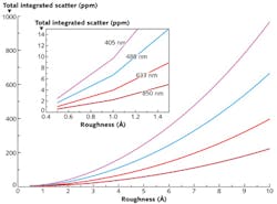
Scattering losses due to surface roughness can be readily understood based on a theoretical calculation of the total integrated scatter (TIS) from a surface having RMS roughness d. The total integrated scatter is exponentially dependent on the square of the ratio of the RMS roughness to the wavelength (l):
TIS = 1 – exp[-(4pd/l)2]
In addition to losses associated with scattering effects, absorption losses must also be minimized and controlled. Light absorption is an intrinsic effect governed by the electronic structure of a specific material. As a result, it is important to select the right dielectric material pairs that provide optimal high-low index contrast (nH/nL) without leading to excessive light absorption over the range of wavelengths over which the mirror must operate efficiently.
The refractory oxides silicon dioxide (SiO2) as the low-index material, and titanium dioxide (TiO2), hafnium dioxide (HfO2), and tantalum pentoxide (Ta2O5) as high-index materials are common choices for hard-coated dielectric mirrors and can be used to provide high index contrast and low absorption loss in the UV to mid-IR range of wavelengths. Fluorides and amorphous semiconductors like silicon (Si) and germanium (Ge), as well as III-V and II-VI compounds, provide for an extended range of operation into the deep-UV or far-IR regions.
Absorption losses can also be affected by imperfect stoichiometry, the presence of chemical impurities, and nonlinear optical processes at high laser intensities, with the last being difficult to control as it is ultimately user-dependent. Variations in stoichiometry can be controlled by selecting the most suitable deposition process, while contributions that result from chemical impurities can be quelled by enforcing the highest quality-control measures to ensure that only the highest-purity starting materials are used.
As described, the ability to control and minimize the primary sources of absorption loss is relatively well understood. What makes achieving low loss so challenging in practice is the difficulty of accurately measuring these losses at the part-per-million level.
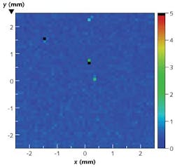
One way to achieve this is to use photothermal common-path interferometry (PCI). A photothermal common-path interferometer consists of two laser sources, a probe beam (typically 633 nm), and a pump beam that are spatially overlapped at the mirror surface, with the wavelength of the pump beam chosen based on the spectral range over which the mirror is designed to operate. In PCI, absorption of the pump beam causes local heating in the mirror. This heating leads to a small, yet measurable phase distortion in the probe beam that is measured as an intensity change in the detector arm of the interferometer. Point-by-point or continuous scanning measurements can be used to generate spatial maps of absorption “hot spots” across a mirror surface (see Fig. 4).Transmission losses also require careful consideration. Like mirror reflectivity, the transmission properties of the mirror coating are controlled and optimized through the design of the multilayer stack and can in essence be made arbitrarily small. However, in most applications some transmission loss is necessary to allow light to be detected as part of the measurement process. A classic example of where a small amount of loss is necessary is in the output mirror of a laser cavity. In many practical applications, mirrors are designed such that T = S + A.
High-reflectivity, low-loss hard-coated dielectric mirrors are a key enabling technology in a wide variety of high-sensitivity optical measurement instruments. Key factors underlining recent advances in mirror performance are the use of super-polishing techniques to minimize and control scattering losses, coupled with the implementation of state-of-the-art IBS deposition processes to reliably and repeatedly manufacture mirrors having R >99.999%, and scattering and absorption losses at the part-per-million level.
As a direct result of these advances, several high-precision, high-sensitivity optical measurements techniques have benefited. One important example is the development of CRDS instruments that are capable of detecting chemical species and quantifying their concentration at the part-per-billion level and below.
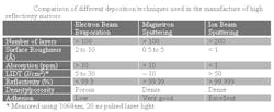
Sputtering techniques such as magnetron and IBS have several distinct advantages over evaporation-based approaches, and are the preferred choice for manufacturing high-reflectivity, low-loss mirrors. Because the material atoms and molecules are deposited at high energy (~10 eV), densely packed layers are formed. This results in mirror coatings with extended lifetimes that are chemically inert and mechanically stable under a wide variety of environmental conditions. Another important aspect that differentiates sputtering from evaporated deposition techniques is the ability to precisely monitor and reliably control the thickness of each individual layer throughout the entire deposition process. In this way, it is possible to reliably and repeatedly manufacture multilayer mirror coatings with spectral performance characteristics that remain true to the initial design.
Generally speaking, IBS holds several advantages compared to magnetron sputtering and is the premier choice when high-reflectivity, low-loss coatings are a must. Because the target is electrically active in magnetron sputtering, arcing—which is characterized as intense localized concentrations of plasma—can lead to the ejection of molten micron-sized particles. Due to the small (~10 cm) gap between the target and substrate, the ejected particles can fall directly onto the substrate and cause defects, such as pinholes, that increase both scattering and absorption losses. This is not the case for IBS. In IBS, the ion beam is electrically neutral and so the coatings do not suffer from the same damaging byproducts caused by arcing that are common to magnetron sputtering.
Additional advantages of IBS over magnetron sputtering center on the fact that the IBS process can be used to deposit very high-layer-count (>200) coatings that exhibit laser-induced damage-threshold values in excess of 20 J/cm2. Furthermore, IBS coatings generally do not exhibit structure and can be used to produce mirrors with extremely low levels of scatter. As such, IBS is the preferred choice for manufacturing high reflectivity, low loss dielectric mirrors. A comparison between evaporation and sputtering techniques is seen in the table.Mirrors for cavity ring-down spectroscopy
There exist several interesting applications where high-reflectivity, low-loss mirrors are critical. One that has benefited greatly from advances in hard-coated dielectric mirrors is cavity ring-down spectroscopy (CRDS), an ultrasensitive spectroscopic technique that is commonly used in the quantitative analysis of trace gas species in environmental and industrial sensing applications. For example, CRDS has been used to measure carbon isotope ratios in archaeology and ecology, extremely low levels of trace water in light-emitting diode (LED) manufacturing, and levels of important greenhouse gas species, such as carbon dioxide.
In CRDS, an optical resonator (cavity) is formed using two or more high-reflectivity mirrors. A laser beam is allowed to enter the resonator and bounce back and forth between the mirrors. In this way it is possible to build a cavity with an effective path length (Leff) on the order of several kilometers within a physical footprint of less than 50 cm. One of the high-reflectivity cavity mirrors is designed to transmit a small fraction of the laser light during each round trip. The emitted light decays exponentially with time and is measured by a photodetector placed in the output arm of the instrument. The decay time (t) depends on several instrument parameters and is given by the following equation (for an empty cavity):
tempty = L/c(1 – R)
where L is the length of the cavity formed by the two high-reflectivity mirrors having reflectivity R, and c is the speed of light. If an absorbing medium is placed within the cavity the decay time then becomes:
t(n) = L/c(1 – R + s(n) NLeff)
where Leff is the effective length of the cavity, s(n) is the cross-section (cm2), N is the number density (molecules/cm2), and n = c/l. These two equations can then be used to determine the concentration of the absorbing species via:
N = (1/cs(n))(1/t(n) – 1/tempty)
In a typical CRDS experiment, all of the instrument and sample parameters, L, c, s(n), are fixed or known, leaving the mirror reflectivity R as the main variable with which to alter the overall instrument sensitivity. In applications where it is necessary to measure molecular species at very low concentrations, mirrors having R = 99.998% or greater are required to enable the detection of gas-phase molecular species at the part-per-billion level, and even the part-per-trillion level.
REFERENCES
1. G. Rempe et al., Opt. Lett., 17, 5, 363 (1992).
2. Light Scattering and Nanoscale Surface Roughness, A.A. Maradudin, ed., Springer Science (2007).
Neil Anderson | Technology Development Analyst, Semrock
Neil Anderson is a technology development analyst with Semrock, a unit of IDEX Optics & Photonics (Rochester, NY).
Ramin Lalezari | President, Advanced Thin Films
Ramin Lalezari is president of Advanced Thin Films, a unit of IDEX Optics & Photonics (Boulder, CO).


