CCDs: Three-chip color CCD captures more accurate surface profiles

For obtaining precise surface profiles quickly over a large area, optical scanning interferometry cannot be surpassed. As long as the surface under test is reflective enough and does not stray too far in shape from the wavefront of the interferometric beam, information over the whole field can be captured at once. However, if the surface under test contains discontinuous structures such as steps, a phase ambiguity remains if only a single wavelength is used. Such surfaces are becoming ever more important: The development of integrated photonics and microelectromechanical systems (MEMS) devices can both benefit from precise measurements of heights and microprofiles of various fabricated objects.
White-light or multiwavelength interferometric surface profilometers solve this phase ambiguity by capturing multiple data points at each measurement location, allowing the relative phase across a step to be determined. Various forms of white-light scanning interferometer (WLSI) are based on the use of a color sensor (usually a CCD camera). However, a single-chip color CCD camera has limitations: For one, each of its pixels measures only an intensity on one channel, with the rest of the values produced through an electronic spatial color interpolation.
Engineers at the National University of Singapore and the Nanjing University of Science and Technology (Nanjing, China) have simulated, fabricated, and tested a WLSI that uses a three-chip color CCD, which correctly records the actual color information.1 (In a three-chip color CCD, a trichroic beamsplitter prism divides the incoming white-light beam into blue, green, and red channels, which are each measured by an individual CCD array.)
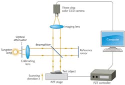
The layout of the instrument is typical of a Michelson-type WLSI (see Fig. 1). The light source is a tungsten lamp; its output is focused into an optical fiber (not shown in the figure) and guided to the focal position of the collimating lens. An attenuator modifies the spectral energy distribution, boosting the signal-to-noise ratio of the blue channel by evening out the intensity of the three colors. The surface under test is placed on a piezoelectric PZT (lead zirconate titanate crystal-driven) stage, which is computer-controlled. The setup has a scanning resolution of 1 nm and a repeatability of better than 0.02%. The three-chip camera is a commercial device produced by JAI (Valby, Denmark) with 1035 × 780 pixels per color and operates in a linear and unsaturated regime in the instrument.
Simulations
The researchers simulated the setup, with some approximations. A two-dimensional 128 × 128 pixel area containing two flat-top rectangular objects 0.013 and 0.028 µm in height was used, along with a simulated light source with a Gaussian spectrum; center wavelengths for the channels were 600, 520, and 450 nm. A scanning interval of 0.05 µm and a scanning range of 10 µm were chosen. The researchers added random intensity noise that they could vary from 0% to 25% of the total intensity.
Two types of interferogram-analysis algorithms were examined: a phase-crossing method with a fast Fourier transform (FFT) using information from only two channels (the green and the blue), as do some pre-existing white-light interferometers; and the researchers’ chosen windowed Fourier transform (WFT), which uses information from all three channels. The modeled RMS profile error for the WFT was far lower than that for the FFT as a function of random intensity noise: For example, at a 25% noise level, the WFT and the FFT show 0.27 nm and 1.86 nm RMS error, respectively. An additional analysis showed that any color-coupling effect related to the three-chip camera was small enough (0.08 nm) that it could be ignored.
Experiment
Because the researchers were more concerned with characterizing the accuracy of measurement along the scanning axis than with accumulating voluminous amounts of lateral data, they reduced the number of pixels from 1035 × 780 to 207 × 156 by resampling the images using only 20% of the pixels. As a result, computing time for a single set of profile data using MATLAB software from The MathWorks (Natick, MA) was reduced to about five minutes on a 3.16 GHz computer with a Core 2 Duo processor.
The researchers started by testing a flat mirror with an RMS height of 0.51 nm and a convex wafer with peak-to-valley (PV) and RMS values of 70 and 15.1 nm, respectively. Deviations were 11% and 16.5% for PV and RMS errors respectively for FFT, and 4.3% and 2.6% for PV and RMS errors respectively for WFT. These errors were mainly due to vibration of the light source.
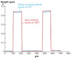
The true test came with the measurement of a MEMS wafer. Here, several cross-shaped features of various lateral sizes ranging from about a hundred to a few hundred microns, all with a nominal height specified at 450 nm by the MEMS wafer manufacturer, were measured. Height data across an area approximately 700 × 950 µm in size were taken, from which profiles could be extracted (see Fig. 2).The average height of the features analyzed by FFT was 441.8 nm with a deviation of 8.2 nm, or a 1.8% relative error, while that obtained by WFT was 446.5 nm with a deviation of 3.5 nm, or a 0.8% relative error. The WFT method also obtained profiles of narrow objects that more truly captured their actual flat tops.
REFERENCE
1. S. Ma et al., Appl. Opt., 50, 15, 2246 (May 20, 2011).

John Wallace | Senior Technical Editor (1998-2022)
John Wallace was with Laser Focus World for nearly 25 years, retiring in late June 2022. He obtained a bachelor's degree in mechanical engineering and physics at Rutgers University and a master's in optical engineering at the University of Rochester. Before becoming an editor, John worked as an engineer at RCA, Exxon, Eastman Kodak, and GCA Corporation.
