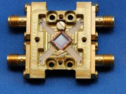
ASTRONOMY: Superconducting focal-plane array spans UV to near-IR
A superconducting array of cryogenic microwave kinetic inductance detectors (MKIDs) is the basis of a photon-counting focal-plane array developed by researchers at the University of California–Santa Barbara (UCSB) and the NASA Jet Propulsion Laboratory (JPL; Pasadena, CA) that operates from the UV to the near-IR.1 Because the MKID arrays have virtually no false photon counts and can determine the time of incidence and approximate wavelength of the photons it receives, the researchers believe the array could replace most semiconductor detectors (such as CCDs) for use in astronomical imaging.
In an MKID, an incident photon changes the surface impedance of a superconductor in a resonator; the photon changes the phase and amplitude of a microwave probe signal tuned near the resonant frequency. Each pixel in the MKID array is fabricated to tune to a different frequency; all signals from different pixels can be separately recovered with little crosstalk by using a frequency comb of probe signals.
32 × 32 superconducting pixels
The researchers created an optical lumped element (OLE) design in which the resonator consists of a 20 nm substoichiometric titanium nitride (TiN) film with a superconducting transition temperature of about 800 mK. Two feedlines that read out the array each serve 512 resonators, which have resonant frequencies in the 4–5 GHz band and are separated from each other by 2 MHz. A “double meander” inductor design precisely cancels out the electric fields from the electrical charges in the sections of the meander.
A rectangular array of circular microlenses with a 100 μm spacing (see figure) focuses the light onto the superconductor with a fill factor of 67% (square lens elements would boost this to at least 95%). Shape optimizations such as tapered resonators ensure uniform responsivity to photons across the resonator. A microwave high-electron-mobility transistor (HEMT) with a 4 K noise temperature amplifies the signal.
For a first experiment, the resonators were illuminated by light at a 254 nm wavelength from a mercury-vapor lamp. The pulse from a single photon has a fall time of about 50 μs, limiting the maximum count per pixel to about 2000 counts/s. The dominant noise source was the HEMT amplifier; reduction of the amplifier noise temperature to something below 4 K should improve the energy resolution.
In a typical 32 × 32 pixel device, about 85% of the resonators were usable, due to fabrication errors causing nonuniformities in the thickness of the TiN film and overlapping resonator frequencies. Future improvements in fabrication will reduce the numbers of overlapping resonator frequencies. Quantum efficiency as a function of wavelength was gauged by measuring the reflection and transmission of a 40 nm TiN film as a function of wavelength with a spectrometer to determine the fraction of photons absorbed in the superconducting film. The approximate measurement (which ignores losses such as due to the microlens array) showed that quantum efficiency approached 80% at 200 nm but dipped to about 30% at 1 μm.
REFERENCE
1. B.A. Mazin et al., Opt. Exp., 20, 2, 1503 (Jan. 16, 2012).

John Wallace | Senior Technical Editor (1998-2022)
John Wallace was with Laser Focus World for nearly 25 years, retiring in late June 2022. He obtained a bachelor's degree in mechanical engineering and physics at Rutgers University and a master's in optical engineering at the University of Rochester. Before becoming an editor, John worked as an engineer at RCA, Exxon, Eastman Kodak, and GCA Corporation.
