PHOTONIC FRONTIERS: GRAPHENE: Graphene photonics are making their way to practical use

Graphene is amazing stuff. Flat sheets of carbon a single atom thick arranged in hexagonal arrays, graphene is the fundamental building block of graphite, a material we take for granted. Yet when prepared properly in the laboratory, graphene has exceptional physical, electronic, and optical properties. Research has snowballed. The journal Nature reported that well over 4000 papers on graphene were published last year. Forty of the more than 650 sessions at the American Physical Society's March 2012 meeting in Boston were devoted to graphene, and some of them were packed.
The initial wave of interest focused on graphene's fundamental physics and potential electronics applications. Now that interest has spread to photonic applications, including transparent conductors for touch screens and electrical contacts on solar cells, saturable absorbers, modulators, and plasmonic devices.
Graphene basics
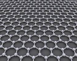
The carbon atoms in graphene arrange themselves in planar hexagonal patterns, with each atom sharing hybrid bonds with its three closest neighbors, as shown in Fig. 1. Two-dimensional sheets bond to each other only weakly, making graphite a soft material. When Andre Geim and Konstantin Novoselov isolated high-quality few-layer graphene in 2004 at the University of Manchester (Manchester, UK), they found graphene sheets had properties quite different than bulk graphite. Single-layer sheets are even more different.Mechanically, graphene sheets are orders of magnitude stronger than silicon or steel, and almost as stiff as diamond. Electrons act as if they are massless in graphene, making their mobility more than an order of magnitude higher than in gallium arsenide (and two orders of magnitude higher than in silicon). Graphene's thermal conductivity is more than a factor of 10 higher than silver. It's no wonder researchers are studying basic physics as well as potential applications.
Graphene also has unusual optical properties. It lacks a natural bandgap, so absorption is uniform across the optical part of the spectrum, from ultraviolet (UV) well into the infrared (IR). That absorption is significant—about 2.3% per layer, enough to make a single atomic thickness visible to the eye. Graphene also displays nonlinear effects such as saturable absorption. Together with its mechanical and electronic properties, that makes graphene attractive for many photonic applications, Andrea Ferrari and colleagues at the University of Cambridge (Cambridge, UK) argued in an influential 2010 review paper in Nature.1 "Until that time, most people were only obsessed about the electronic properties of graphene," recalls Ferrari, but now many are investigating potential photonic applications.
Strong, transparent, conductive, and cheap
A wide range of consumer products could benefit from graphene's combination of strength, transparency, and conductivity. Today's smart phones and tablet computers use touch screens covered with transparent electrodes made of indium tin oxide (ITO). Yet ITO has major limitations. Indium is a scarce material that is already expensive, and its price will rise further with demand. ITO is brittle and requires a rigid substrate such as glass, so it can't be used in flexible displays or on screen materials such as organic LEDs.
A single layer of graphene transmits more than 97% of incident light, well above the 90% of ITO, and graphene's strength and flexibility make it attractive for flexible screens. Single-layer graphene is less conductive than ITO, but adding layers increases conductivity—although at the cost of lower light transmission. However, graphene's biggest advantage could be that it does not require costly raw materials; carbon is abundant, so efficient manufacturing could make graphene cheap.
Transparent conductors could be the first commercial application for graphene, says Tony Heinz of Columbia University (New York, NY). It can't be deposited in the same way as ITO, but developers are working on other fabrication processes.
Saturable absorption and modelocking
Another photonic property of graphene well on its way to applications is its strong third-order nonlinearity, a property it shares with carbon nanotubes. Saturable absorption and passive modelocking, which arise from third-order nonlinearity, were first reported in nanotubes in 2003, and first observed in graphene in 2009.
In hindsight, that should not be surprising; nanotubes are sometimes considered as essentially rolled-up sheets of graphene. However, at the time it surprised many observers, as Shinji Yamashita of the University of Tokyo (Tokyo, Japan) observed in a tutorial on the nonlinear properties of graphene.2 He and others had assumed that fast saturable absorption in nanotubes was due to their unusual one-dimensional structure. Yet, he wrote, "once demonstrated, graphene looked more promising...due to its wavelength-independent optical absorption." Since then, graphene modelocking has been shown to produce femtosecond soliton pulses, nanojoule solitons, dissipative solitons, and repetition rates to 10 GHz in solid-state or fiber lasers.
Waveguide modulators
Electro-optic modulators are another possible application. Graphene is a thin material with a low density of states, so changing the Fermi energy—the boundary between occupied and empty states—can change its transitions and thus its transparency. The modulation effect spans a broad range of wavelengths, although the absorption of a single atomic layer of graphene is only a few percent. However, Heinz says, "it's clear that you can also adapt graphene for a waveguide configuration," producing a much longer interaction length and much greater modulation depth.
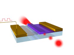
Last year, Feng Wang's group at the University of California (Berkeley, CA) made just such an integrated graphene waveguide modulator operating at wavelengths of 1.35 to 1.6 μm, shown schematically in Fig. 2. They reported modulating the graphene's transmission at frequencies to 1.2 GHz.3 Occupying an area of only 25 μm2 on the chip, the active graphene device had a volume orders of magnitude smaller than conventional semiconductor modulators. An important advantage of the new modulator, the Berkeley group reported, is that it is compatible with CMOS processing techniques.Detectors and plasmons
Pure graphene lacks the bandgap found in semiconductors, which can limit some photonics applications. However, because graphene has a zero bandgap it absorbs light at a broad range of wavelengths out to the far infrared (IR) and terahertz bands, which could fill important holes in the detector spectrum. Many groups have reported encouraging results on graphene detectors, although the underlying mechanisms remain under investigation. Many of the detectors appear to be bolometric, based on changes in resistance induced by heating the low-thermal-mass graphene rather than photon detectors.
Some detectors go deep into the far-IR. Wang's group at Berkeley has detected wavelengths to hundreds of microns with an array of 4-μm-wide graphene ribbons. At that wavelength, the structures form a metamaterial, which detects the effects of the long-wavelength radiation by its effects on plasmons in the graphene.4 Changing the size of the ribbons or applying an electrostatic charge can tune the wavelength.
Plasmonics has been developing very rapidly in the past couple of years, aided by the high carrier mobility in graphene. "These excitations occur at long wavelengths, so you need reasonably big samples" to study them, says Heinz. That has been aided by new chemical-vapor deposition techniques that can grow graphene in larger sizes. Experimentalists want to test theoretical predictions of long-distance propagation and very high Q resonances of surface plasmons in graphene.
Outlook for graphene
Plasmon research is part of a broad trend. "There is tremendous growth in graphene photonics," says Ferrari. "We are at the beginning of exponential growth." Improved fabrication methods are making graphene available in larger quantities and better quality for developers, and that enhanced production is an important step toward practical applications of the material.
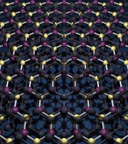
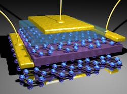
New ideas continue to appear. Early this year, Geim and Novoselov's group at Manchester reported making a field-effect transistor in graphene that by adding a layer of boron nitride to form vertical heterostructures, shown schematically in Fig. 3.5 They wanted the heterostructures so the transistor could serve as a switch, but heterostructures have a broad importance in photonics as well as electronics because they add a bandgap to the device, which in principle can be tailored to the application. BN has a deep-UV bandgap, but molybdenum sulfide can form similar layers and has an IR bandgap "ideal for photonics applications including lasers and detectors," says Ferrari. The invention of heterostructures in the 1960s laid the groundwork for huge advances in diode lasers.Graphene has come a long way from the days when it was a couple of guys studying layers they pulled off graphite with sticky tape. That work earned Geim and Novoselov a Nobel Prize in 2010. We're likely to be reading a lot more about graphene photonics in coming years.
REFERENCES
1. F. Bonaccorso et al., "Graphene photonics and optoelectronics," Nat. Photon., 4, 611 (Sept. 2010).
2. S. Yamashita, "A Tutorial on Nonlinear Photonic Applications of Carbon Nanotube and Graphene," J. Lightwave Technol., 30, 427 (Feb. 15, 2012).
3. M. Liu et al., "A graphene-based broadband optical modulator," Nat., 474, 64-67 (June 2, 2011); doi:10.1038/nature10067.
4. L. Ju et al., "Graphene plasmonics for tunable terahertz metamaterials," Nat. Nanotechnol., 6, 630-634 (2011).
5. L. Britnell et al., "Field-effect tunneling transistor based on vertical graphene heterostructures," Sci., 335, 947 (2012); doi: 10.1126/science.1218461.

Jeff Hecht | Contributing Editor
Jeff Hecht is a regular contributing editor to Laser Focus World and has been covering the laser industry for 35 years. A prolific book author, Jeff's published works include “Understanding Fiber Optics,” “Understanding Lasers,” “The Laser Guidebook,” and “Beam Weapons: The Next Arms Race.” He also has written books on the histories of lasers and fiber optics, including “City of Light: The Story of Fiber Optics,” and “Beam: The Race to Make the Laser.” Find out more at jeffhecht.com.


