HIGH-SPEED IMAGING: Digital image correlation measures 3D surface deformation
ANDREW BRIDGES and ALISTAIR TOFTS
Digital image correlation (DIC) is a noncontact measurement technique that uses high-resolution machine-vision digital cameras to accurately measure surface deformation in two or three dimensions. Early development of this technology began in the mid-1980s in the mechanical engineering department of the University of South Carolina (Columbia, SC).
Because digital cameras were virtually nonexistent in the 1980s, researchers and PhD candidates began converting images from film photography to digital images using high-quality scanners. The digital image produced from a photograph could then be used to test matching algorithms for measuring 2D surface displacements, and eventually strain, although the process was extremely slow.
The vast hardware improvements since then include machine-vision digital cameras with much higher resolutions, lower noise levels, and faster acquisition rates, and much faster and more efficient computer central processing units (CPUs). These allowed engineers to develop more robust and faster DIC algorithms, while researching and improving specimen-preparation techniques to achieve the best spatial resolution. The next step was to use two digital cameras at once to measure 3D surface deformations. In 1998, the first commercial turnkey 2D and 3D DIC systems became available through Correlated Solutions, a newly founded company at that point.
The basics
When a product is in the design stage, it is important for the engineer to come up with a robust design using the most cost-effective material without sacrificing features or safety requirements. Regarding mechanical properties, the first step is to create a 3D computer-aided design (CAD) model and perform a finite-element analysis (FEA), which tells the engineer, in theory, where the stress concentrations should be located, and where the failure point "should" be under a certain loading condition.
To validate the computer model, engineers typically place strain gauges in the predicted high-stress locations on a test specimen, apply a force in the same location and direction as the model, and then analyze and compare the strain data from the strain gauges to the theoretical data from the FEA model. Typically they do not match, and engineers have to determine how to adjust the test (or the computer model) so that the results make sense.
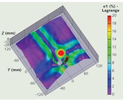
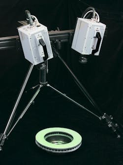
Digital image correlation eliminates this lengthy process by measuring the displacements and strains over the entire surface of the specimen so precise gauge placement is not required. The end result is a full-field 3D displacement and strain measurement of the specimen's surface (see Fig. 1). Validating theoretical computer models is an essential step to designing a quality product with an efficient use of materials. DIC makes this process much faster by providing richer data at higher rates. One of the many key advantages to DIC systems is the fact that it measures full-field 3D surface strains over the entire specimen's geometry without any mechanical interaction with the sample, eliminating the need for strain gauges and saving many man-hours (see Fig. 2).High-speed DIC
Over the years, DIC has found widespread popularity in many quasi-static applications due to its robustness, flexibility, accuracy, and overall ease of use. Although DIC has traditionally been used mostly for quasi-static or moderately dynamic applications, the availability of affordable high-speed and ultrahigh-speed cameras over the recent years has led to a dramatic increase in the use of DIC systems for dynamic applications.
Because of its noncontact measurement principle and high spatial resolution, DIC can provide unprecedented measurement capabilities at high loading rates. Applications range from coupon-level testing (tests done on samples of the material) to characterizing rate-dependent material properties, as well as the dynamic characterization of complete structures under high rate loading conditions.
Many times, the former end of the application spectrum is driven by the need for accurate material parameters as an input for FEA models, while the latter end is driven by the need for FEA model validation. In either case, a pair of synchronized images provided by two cameras is analyzed by software to produce a 3D strain field (see Fig. 2).
Today, high-speed cameras predominantly use CMOS sensors. This change is a result of significant improvements in cost over the older CCD technologies, which were traditionally used for high-speed imaging. CMOS sensors are fabricated on a single piece of silicon with the control and support circuitry incorporated onto the sensor as opposed to requiring a separate circuit, as was usually the case with CCD cameras.
The issues of noise have been overcome in modern CMOS sensors, and the lower power consumption of CMOS technology brings further benefit to this type of sensor. Certain specialized cameras still use CCD technology, but this is due to the in situ image storage (ISIS) CCD architecture, which permits the storage of pixel information on the chip itself to produce full-resolution framing speeds as high as 1 million frames/s.
One of the biggest advantages of CMOS sensors is that they do not suffer from blooming (also called tearing). This is where the brightest parts of an image result in electrons (converted from photons hitting the CCD pixels) leaking from the charge-holding region and spilling onto neighboring pixels, resulting in vertical streaks emanating above and below the bright spot. CMOS sensors have better antiblooming characteristics, as well as improved power consumption and speed, because they convert their resultant electron charge to a voltage on the pixel itself, negating the need for shift registers and complex clock timing and voltage biases.
High-speed CMOS sensor sensitivity has also improved dramatically over what it was when it was first introduced about ten years ago. The earliest CMOS cameras required so much light that there existed the very real danger of the subject spontaneously combusting due to the heat generated by several kilowatts of lighting bearing down on a small area. Today, high-speed cameras are much more light sensitive; this is due to significantly improved fill factors (the amount of physical real estate actually dedicated to gathering light as opposed to the control electronics) and the use of microlenses to focus the maximum quantity of light onto these light-sensitive parts of the pixel.
System considerations
Unfortunately for prospective buyers, certain ways exist of measuring a digital camera's light sensitivity that can result in some pretty outlandish claims. For example, if an ISO rating of greater than 30,000 is claimed for a monochrome camera and one-half to one-third that for the color equivalent, one should be highly skeptical. Most reputable camera manufacturers have adopted the ISO 12232 Ssat method, whereby the entire camera's sensitivity, as opposed to that of the sensor by itself, is measured at the 100% white exposure point immediately before any blooming occurs. As with all measurements, there is still some room for (mis)interpretation, so for best results an "apples to apples" comparison should be made by requesting a live demonstration.
Digital image correlation requires very precise camera synchronization to provide the tightest possible tolerances for spatial and temporal displacement calculation. An example high-speed camera has megapixel resolution (1024 horizontal by 1024 vertical pixels) at rates up to 12,500 frames/s and precise synchronization to other cameras or signal sources such as lasers, external signal generators, or satellite time codes (see Fig. 3). The camera can also act as a delay generator, with a resolution of x nanoseconds between synchronization signals, regardless of whether the signal source is another high-speed camera, a laser, or some other data-acquisition system.Another critical consideration is the shutter time, or the time during which the pixels are globally exposed per frame. Note the use of the word "globally," meaning that all pixels are exposed at the same time, as opposed to row by row. Shutter time is not to be confused with framing rate, which is the number of frames the camera takes in any given second. A faster shutter time will require more light because the pixels are exposed for less time, but it will reduce or remove any blur present in the image.
Blur is a hindrance when an engineer is trying to accurately track very small points that are moving very rapidly from frame to frame. Establishing the maximum (longest) acceptable shutter time requires the engineer to calculate how far the object points will likely travel between frames, while establishing the optimum frame rate is usually a relatively straightforward matter of calculating the minimum number of samples per second required to discern the motion of the points of interest.
Andrew Bridges is at Photron, 9520 Padgett St., Suite 110, San Diego, CA 92126-4446; www.photron.com. Alistair Tofts is at Correlated Solutions, 120 Kaminer Way Pkwy A, Columbia, SC 29210; www.correlatedsolutions.com. E-mails: [email protected] and [email protected].


