NANOPHOTONIC SENSING: Silicon nanowire arrays form color-coded refractive-index sensors

A variety of silicon-nanowire-based devices have been developed in recent years due to their unique optical properties: namely, individual nanowires can confine carriers and photons in the transverse plane while allowing them to propagate longitudinally, and nanowire arrays have unique absorption and reflection properties with customizable bandgaps.
While silicon (Si) nanowires and arrays based on plasmonic interactions and fluorescence have been used in sensing applications, the methods typically involve expensive imaging spectrometers and light sources to measure spectral changes. But researchers at the University of Waterloo (Waterloo, ON, Canada) are combining a recently discovered property of vertical Si nanowire arrays—color reflection—with fluids as the surrounding substrate to create an inexpensive, effective refractive-index sensor.1
Array coupling and reflection mechanisms
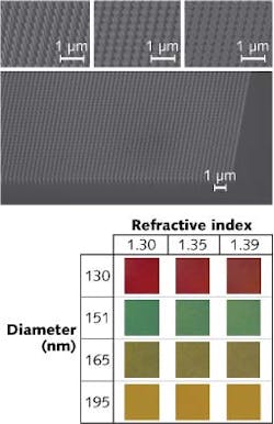
Using electron-beam lithography and inductively coupled plasma-reactive-ion etching, arrays (100 × 100 μm) of vertically aligned Si nanowires (typically 1 μm long) were fabricated in square lattices with nanowire diameters ranging from 105 to 346 nm with a 400 nm pitch on silicon-on-insulator (SOI) substrates (see figure). Depending on the array configuration and nanowire diameter, different colors are reflected that span the entire visible spectrum.
Using ellipsometry and other spectral and polarization instrumentation, research shows that the nanowire arrays act like 2D dielectric gratings, supporting guided slab modes that result in resonant coupling between the incident wave and guided modes. The different diffraction orders create different reflected colors that are also influenced by the length and diameter of the nanowires, as well as the air-nanowire and nanowire-SOI substrate interfaces, which create a Fabry-Perot cavity.
By introducing fluids with varying refractive indices into the arrays as an additional substrate, further Fabry-Perot cavity interactions cause more subtle color variations in the reflected signature. Using Cargille (Cedar Grove, NJ) refractive-index fluids with index values ranging from 1.3 to 1.39 as the substrate within arrays of varying nanowire diameter, color changes were more pronounced for some nanowire diameters (130 and 150 nm) and weaker for others (165 and 195 nm).
Sensor effectiveness
Refractive-index variation is correlated to color using only a camera with a CCD sensor and simple image processing using an additive RGB (red, green, blue) model. For a 130-nm-nanowire-diameter array, the best refractive-index resolution was 5 × 10⁻⁵, although typical resolutions are in the 1 × 10⁻⁴ range and comparable to more complex and expensive integrated-optics-based sensors. Furthermore, the color change is nearly insensitive to temperature changes in the test environment—an important attribute for any optical sensor.
“Low-cost measurements in optics are the holy grail for photonics researchers,” says researcher Simarjeet Singh Saini. “Our group here at the University of Waterloo is very excited about our proposed nanowire sensors which create colors similar to those seen in butterfly wings. Our focus now is to increase the sensitivity of our CMOS-compatible sensors, and early results are showing that different lattice arrangements can double the demonstrated sensitivity. Other applications including photo imagers and optical filters are also sought after, and with the diversity of talent in the research group, we hope to continue generating new technologies and ideas.”
REFERENCE
1. M. Khorasaninejad et al., Nano Lett., 12, 8, 4228–4234 (Aug. 8, 2012).
About the Author

Gail Overton
Senior Editor (2004-2020)
Gail has more than 30 years of engineering, marketing, product management, and editorial experience in the photonics and optical communications industry. Before joining the staff at Laser Focus World in 2004, she held many product management and product marketing roles in the fiber-optics industry, most notably at Hughes (El Segundo, CA), GTE Labs (Waltham, MA), Corning (Corning, NY), Photon Kinetics (Beaverton, OR), and Newport Corporation (Irvine, CA). During her marketing career, Gail published articles in WDM Solutions and Sensors magazine and traveled internationally to conduct product and sales training. Gail received her BS degree in physics, with an emphasis in optics, from San Diego State University in San Diego, CA in May 1986.