University of California–Berkeley and Lawrence Berkeley National Laboratory (LBNL) researchers have developed a technology that could turn any semiconductor material into a photovoltaic (PV) device, in effect putting bad (and perhaps inexpensive) materials to use. The research broadens the potential for developing low-cost PV devices from earth-abundant, nontoxic semiconductors such as metal oxides, sulfides, and phosphides.
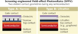
The screening-engineered field-effect photovoltaics (SFPV) technology leverages the electric-field effect in which the concentration of charge carriers in a semiconductor is altered by an applied electric field. Using only electrode and gate deposition (rather than high-temperature, expensive, and damaging chemical doping or ion implantation), a geometrically structured partially screening top electrode allows the electric field to penetrate the electrode and modulate the semiconductor carrier concentration and type, inducing a p-n junction.
In a copper oxide structure (Type A), the electrode contact was shaped into narrow fingers; in another configuration with silicon (Type B), the top contact was single-layer graphene. Both create high-quality p-n junctions. Other tailored variations could turn virtually any semiconductor into a PV device. Contact Alex Zettl at [email protected].

Gail Overton | Senior Editor (2004-2020)
Gail has more than 30 years of engineering, marketing, product management, and editorial experience in the photonics and optical communications industry. Before joining the staff at Laser Focus World in 2004, she held many product management and product marketing roles in the fiber-optics industry, most notably at Hughes (El Segundo, CA), GTE Labs (Waltham, MA), Corning (Corning, NY), Photon Kinetics (Beaverton, OR), and Newport Corporation (Irvine, CA). During her marketing career, Gail published articles in WDM Solutions and Sensors magazine and traveled internationally to conduct product and sales training. Gail received her BS degree in physics, with an emphasis in optics, from San Diego State University in San Diego, CA in May 1986.
