DETECTORS: Balancing sensor parameters optimizes imaging device performance
BEHNAM RASHIDIAN
The objective of a vision system can be summed up as providing the right image (image quality) at the right time (imaging speed) and place (device interface image data rate). System architects strive to balance various specifications and performance matrices, specifically those related to the imaging device, to achieve the best inspection system accuracy and speed, within budget constraints.
Imaging device attributes such as speed, noise, and sensitivity must be harmonized with other attributes, such as available light intensity and pixel charge capacity. A narrow view emphasizing only a subset of these parameters may mislead the system architect into a suboptimal imaging system design.
Some attributes of the imaging device are more important in certain applications. For example, in low-light scientific imaging applications the noise floor of the imaging device is critical, whereas the charge capacity of the device is less important. In contrast, in typical industrial applications where the illumination is not so constrained, the full well capacity of the sensor plays a more significant role in the final image quality.
The relationship between major specifications of an imaging device—whether CCD or CMOS sensor—and how these attributes impact final image quality and speed of the device are the subjects of this article. The seven major attributes to be discussed are available light illumination, pixel charge capacity, speed, sensitivity, pixel digitization, and noise, as well as how these attributes impact signal-to-noise ratio (SNR).
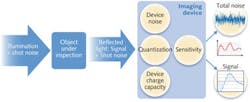
Figure 1 shows a basic representation of a typical imaging system. Incident light on the object is reflected from (or can be transmitted through) the object. This reflected signal is modulated with the image information from the object and constitutes the input signal to the imaging device. Resolution and pixel size attributes—which determine the spatial performance aspect of the imaging device—are not discussed here because these are typically determined by the type of inspection application.
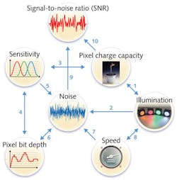
Figure 2 shows the links between the seven attributes (or parameters). These are examined in the following sections (numbers in parentheses for reference to Fig. 2).Starting with the photons
The first step toward great image quality is having great illumination. Generally, more light intensity results in better image quality as long as the vision system can handle it, and this is where the pixel charge capacity comes into play (links 1, 2). The sensor charge capacity must be chosen such that it can store the maximum amount of light available before saturation. Therefore, the amount of light intensity available per image and the pixel charge capacity of the sensor must be chosen optimally.
A sensor with small pixel charge capacity cannot handle all available illumination and results in suboptimal image quality. Available illumination can be increased by changing camera parameters such as exposure time or by upgrading the lighting system to greatly enhance imaging results. In some applications, such as low-light scientific imaging or x-ray, the available illumination intensity is limited and/or cannot be increased.
There are two reasons for desiring maximum possible illumination. When the incident light is reflected from the object under inspection, the image data are carried in the reflected light in the form of spatial contrast modulation. A higher incident light intensity will result in higher spatial contrast in the reflected light intensity.
The second reason for better image quality associated with brighter images is the inherent shot noise characteristic of the incident light. The incident light intensity on any point on the object follows a Poisson distribution and exhibits shot noise characteristics.
Shot noise value is equivalent to the square root of the incident light value, and the SNR of the incident light intensity is the square root of incident light value. In high illumination areas, shot noise dominates all other noise sources—including the noise from the imaging device—and the input image quality will be determined mostly by light intensity. The imaging device must have enough pixel capacity to utilize maximum light available.
Sensitivity, charge capacity, and digitization
In a digital camera, the intensity of each pixel is represented by a digital number (DN) with a range that is determined by the number of bits allocated to each pixel. In an 8 bit data format, the values between 0 and 255 represent the range of light intensity for each pixel. So the sensitivity of the device can be stated in terms of output digital number per unit of input light intensity, typically stated in DN/nJ/cm2, where light intensity is described in nanojoules per square centimeter (links 3-6).
Having two cameras with the same bit depth per pixel, the camera capable of handling higher light intensity will exhibit a lower light sensitivity. Increasing the gain in the camera beyond optimum will lower the effective charge capacity and the maximum light intensity the camera can handle. This will generally result in higher sensitivity at the expense of lower overall image quality due to lower SNR associated with lower light intensity. Increasing sensitivity of a camera by increasing camera gain results in both signal and noise increase and may not improve SNR, but it may improve detectability of certain features in the image.
A higher pixel bit depth is generally associated with lower quantization error of the analog-to-digital conversion process. This error must be very small compared to other sources of noise. As such, increased pixel bit depth benefits systems with lower noise floor. Increasing pixel bit depth beyond a certain number will not contribute to better image quality and will reduce data bandwidth utilization efficiency and limit imaging speed. Light-starved applications, where the absolute system noise value and imaging speed are lower, benefit from higher pixel bit depths. Most scientific applications can benefit from having 16 bit images, whereas typical vision applications need only 8 bit pixel data.
Imaging speed, noise, and illumination intensity
The speed of the imaging system is dictated by many applications themselves. Typically, limitations concern the minimum acceptable speed where a minimum system throughput is targeted. Sometimes, the imaging speed is limited by the type of application and not the camera itself. For example, in low-light scientific imaging, the available light intensity may be the major bottleneck.
The noise in any image has two main components: the inherent shot noise from illumination itself and the noise added by the image sensor acquisition electronics. As the incident light intensity increases, so does the shot noise as well as the signal component that reaches the camera.
The noise contributed by the sensor has two major components: the readout noise and the dark current noise. The readout noise typically increases as the imaging speed increases and the dark current noise increases as the exposure time increases. For each camera, an optimal operation point can be found where the total electronic noise is minimal for certain applications. In high-speed applications, readout noise dominates the electronic noise. In high-intensity applications, illumination shot noise dominates total noise, including readout and dark current noise.
The speed of the camera limits the exposure time available for each image. It is during this maximum exposure time that the brightest pixels in the image must be filled to their maximum capacity. Imaging system illumination must be strong enough to utilize this capacity within exposure time limits imposed by imaging speed.
Pixel charge capacity, total noise, and signal-to-noise ratio
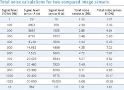
In our simplified linear model of image quality assessment, the quality of the final image of a vision system is mostly determined by two factor: the strength of the output signal and the total uncertainty associated with the measured signal value or total image noise. A common misunderstanding about image sensors is that a sensor with lower noise specification results in a better output image quality. This would be true if all sensors would provide the same level of output signal, but it is not typically the case. To better understand the role of sensor electronic noise and charge capacity in the output image quality, we compare two otherwise identical sensors with different noise and pixel capacity specifications.In this example, we assume a 10 bit per pixel data digitization (0-1023 DN output). Sensor A has a sensitivity of 1 DN per 29 electrons; this figure for sensor B is about 1 DN per 10 electrons. Sensor A has a noise figure of 1.36 DN compared to 1.02 DN noise value of sensor B.
Therefore, sensor B is a more sensitive sensor with lower electronic noise. However, sensor A can handle higher illumination intensity before saturation.
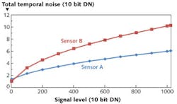
At each output signal level in units of DN (digital number between 0 and 1023), the total noise consisting of the inherent illumination shot noise and the device electronic noise is calculated for each sensor. As we can observe from Fig. 3, sensor B with lower device noise exhibits lower total noise only at very low output signal levels. However, as the signal increases in value, the shot noise in the signal quickly becomes the dominating noise source. Since sensor A can handle higher charge capacity at each digital output number, it shows better signal-to-noise ratio at average signal values just above 12 DN in a 0-1023 DN scale.
The total noise calculations for these two sensors are summarized in the table. It is important to determine where the crossover occurs for each specific application in order to choose the sensor that provides better output image quality.
Behnam Rashidian is a senior product manager at Teledyne DALSA, Waterloo, ON, Canada; e-mail: [email protected]; www.teledynedalsa.com.


