DETECTORS FOR INTEGRATED PHOTONICS: Gain peaking doubles the bandwidth of Ge photodetectors in CMOS
Techniques now exist for greatly increasing the bandwidth of germanium photodetectors fabricated in silicon integrated photonics, taking advantage of newer, more complex structures created via CMOS processes.
Integrated photonic systems based on silicon (Si) can dramatically boost data transmission rates over those for all-electrical transmission. Network and rack-to-rack optical interconnects based on Si photonics are already in use; in development are chip-to-chip and, further out, intrachip Si-based optical interconnects. A powerful motivating force behind Si photonics technology is the ability to fabricate integrated photonic systems using standard CMOS processes commonly used in the electronics industry.
However, neither light emitters nor photodetectors fabricated from Si on Si substrates tend to perform well, so germanium (Ge)—which can also be part of a CMOS-compatible process—is often used as the active component material, integrated into the silicon platform via epitaxy.
For photodetectors, the low absorption coefficient of 0.2 dB/μm for Ge at 1550 nm (the wavelength usually used for Si photonics) results in physically large detectors. Although larger sizes increase responsivity, they also lead to larger parasitic electrical capacitance, which reduces the detector bandwidth. In addition, if bump-bonding is used to bond the Ge component to the Si substrate, the parasitic capacitance is even further increased.
Three types of gain peaking
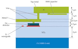
A team of researchers from the University of Washington (Seattle, WA) and the University of Delaware (Newark, DE) has developed an approach to Ge-on-Si detector fabrication that allows for larger detector sizes while reducing the parasitic capacitance.1 The approach, which so far exists only as a simulation, would take advantage of recent fabrication techniques that allow the fabrication of multi-metal-layer devices, such as metal-insulator-metal (MIM) capacitors, adjacent to waveguide-coupled integrated detectors (see Fig. 1).
The researchers' approach is called gain peaking—a technique that is most commonly used by electrical engineers for optimizing the design of amplifiers. There are a number of different types of gain peaking, and the researchers tried out three of them.
The first is called series gain peaking, which produces an increase in detector bandwidth of about 40%. The second involves incorporating an additional capacitor to produce a bandwidth increase of up to 100%. The third, called shunt gain peaking, results in a tradeoff of narrowband operation for a large increase in operating frequency.
Series gain peaking requires the addition of an inductor in series with the load of the photodetector. In one example, a detector with a parasitic capacitance of 35.2 fF and a resistance of 130 Ω has a bandwidth of 25 GHz. Adding an inductor of 0.57 nH (a reasonable value for an integrated inductor) raises the bandwidth to 35.5 GHz.
One thing to watch out for in series gain peaking is the possible introduction of dispersion (differing time delays for differing frequencies). In the example detector, the maximum dispersion is only 0.3 ps at a 30 GHz frequency, which is very small in comparison to the 28.2 ps period of the full 35.5 GHz bandwidth.
In enhanced series gain peaking, an extra parasitic capacitance becomes part of the circuit, either intrinsically (through bump-bonding), or intentionally added by including a MIM capacitor. Though this capacitance would normally detract from the detector's performance, optimizing the added inductor can actually increase bandwidth.
The researchers determined optimal capacitance and inductance values via a two-dimensional gradient that maximizes the 3 dB bandwidth. They calculated such values for detectors with a variety of bandwidths and other characteristics. For example, the 29 GHz bandwidth of one detector was boosted to 57 GHz using this technique—an improvement of 97%. The maximum dispersion for this detector was only 0.6 ps at 46 GHz-again, small in comparison to the period of the full bandwidth.
Shunt peaking
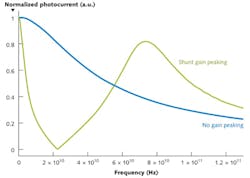
In shunt gain peaking, a detector circuit for a detector operating in only a narrow band can be made to operate at a very high frequency (far above that of a broadband detector) by adding another capacitor to prevent a short circuit at low speeds. In one example, a detector with an unmodified bandwidth of 30.6 GHz can, with proper values for capacitance, resistance, and inductance, be altered to have a bandwidth from 59.1 to 93.4 GHz, peaking at 73.4 GHz with a responsivity of 82% of that at 0 Hz (see Fig. 2).
While inductors are not always easy to add to CMOS integrated circuitry, the inductors required for gain peaking for Ge photodetectors can take a relatively simple geometry, that of a double square spiral taking up a total area 75 × 75 μm square, with a 10 μm width for the spiral trace itself. Most of the spiral is made from the top metal layer, with the single crossover fabricated from the lower metal layer.
The researchers did a noise analysis of the photodetector circuits, especially the combination of parasitic resistance and the inductor, which together produce thermal noise. For the shunt-peaked detector, the ratio of excess noise from shunt-peaking to the load noise was about 0.4 at 80 GHz.
The researchers note these capabilities stem entirely from the complex structures now available in CMOS-compatible Si photonics; taking advantage of them could realistically double Ge photodetector bandwidths with no harmful side effects.
REFERENCE
1. M. Gould et al., Opt. Expr., 20, 7, 7101 (Mar. 26, 2012).
More Laser Focus World Current Issue Articles
More Laser Focus World Archives Issue Articles


