ARTIFICIAL RETINAS: PV retinal prosthesis has high pixel density
Even though age-related macular degeneration and retinitis pigmentosa cause loss of ocular photoreceptors, most of the inner retinal neurons typically survive for a long time. In addition to optogenetic-based therapies, methods to restore sight to the visually impaired typically involve external cameras and implanted wired electrode arrays to stimulate these neurons; however, the required components are bulky, pixel density is low, and the delivered image cannot be scanned naturally by the eye.
Pixel density is much improved in devices that use photosensitive pixels such as those from Retina Implant AG (Reutlingen, Germany); but again, external power delivery makes the device very bulky and greatly complicates implantation and maintenance.
In response to these drawbacks, researchers at Stanford University (Stanford, CA) and the University of California, Santa Cruz have developed wireless, photovoltaically driven, subretinal arrays of photodiodes to stimulate the inner retinal neurons that transmit signals to retinal ganglion cells when illuminated with pulsed near-infrared (NIR) light.1 The scheme eliminates the need for complex electronics and wiring and preserves the natural link between image perception and eye movement.
NIR goggle projection
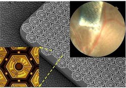
The retinal prosthesis basically consists of a miniature video camera to capture images that are processed by an external computer and projected into the eye via a near-to-eye goggle projection system using pulsed NIR (880–915 nm) illumination. The image is focused on the retina, and the subretinal photodiode array, like any photovoltaic device, converts the light into pulsed photocurrent for neural stimulation at each pixel location (see figure).
Because ambient light is much too dim (by at least a factor of 1000) to photovoltaically stimulate neurons, the NIR laser image projection system produces more intense pulsed illumination that drives the photodiode array. The light-induced temperature rise is kept within the physiological range of ocular safety regulations (less than 1ºC) by limiting the average irradiance to 5.2 mW/mm2 at the 905 nm wavelength used in this part of the study.
High-pixel-density arrays
Each 70 µm pixel contains a photodiode connected to a 20-µm-diameter iridium oxide electrode. Each pixel converts the received light into a charge-balanced stimulation pulse. Corresponding pixel density is about 180 pixel/mm2.
In order to limit the amount of crosstalk between pixels caused by the common return electrode in current array designs, one solution is local return electrodes for each pixel. Three diodes per pixel are connected in series to achieve a higher current density. The triple-diode pixels produce up to 1.5 V at physiologically safe light intensities and require 3X illumination levels for the same current output compared to single-diode pixels.
Laboratory testing using both healthy and degenerate rat retinas implanted with both single- and triple-diode arrays confirmed successful stimulation of the inner retina, with retinal response influenced by the illumination levels and pulse durations. Stimulation threshold (peak irradiance) with 4 ms pulses was 0.3 mW/mm2—more than two orders of magnitude below the ocular safety limit.
The thin (30 µm) and wireless retinal implant drastically simplifies the complexity of subretinal surgery. Multiple modules can be implanted side-by-side to cover a larger field of view. Furthermore, the array is amenable to fabrication on a flexible silicon substrate for easier conformity to eye curvature.
REFERENCE
1. K. Mathieson et al., Nat. Photon., 6, 391–397 (2012).

Gail Overton | Senior Editor (2004-2020)
Gail has more than 30 years of engineering, marketing, product management, and editorial experience in the photonics and optical communications industry. Before joining the staff at Laser Focus World in 2004, she held many product management and product marketing roles in the fiber-optics industry, most notably at Hughes (El Segundo, CA), GTE Labs (Waltham, MA), Corning (Corning, NY), Photon Kinetics (Beaverton, OR), and Newport Corporation (Irvine, CA). During her marketing career, Gail published articles in WDM Solutions and Sensors magazine and traveled internationally to conduct product and sales training. Gail received her BS degree in physics, with an emphasis in optics, from San Diego State University in San Diego, CA in May 1986.
