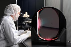
MLD Technologies (MLD; Mountain View, CA) has successfully scaled up an ion-beam sputtering (IBS) deposition process to provide uniform (less than 1% variation), low-loss (less than 15 ppm total loss, defined for mirrors as the sum of absorption loss, transmission loss, and scatter loss) precision optical coatings for large optical substrates up to 500 mm in diameter. Using metal oxides, MLD can deposit optical coatings for use at wavelengths ranging from ultraviolet (UV) to mid-infrared (mid-IR).
MLD brought online two 1.5 m IBS coating chambers equipped with double planetary rotation fixturing that can deposit uniform coatings on two large-diameter optics per processing batch. Large-optics inspection and cleaning facilities were developed to support the coating operation. Metrology instrumentation includes 305-mm-aperture phase-measuring interferometers operating at 1064 nm and 1315 nm, as well as a 305-mm-precision (better than 3 nm rms flatness) reference flat to characterize uncoated substrates and coated optics. Laser-based photometers measure reflection and transmission on the full-size optics at both the design angle of incidence and polarization, and at numerous wavelengths. A large-optics spectrophotometer with a translation stage measures spectral performance over a broad wavelength range. Absorption and optical losses in the coatings can be measured directly with a photothermal common-path interferometer and with cavity-ringdown loss meters. Contact Ric Shimshock at [email protected] or Linda Lingg at [email protected].

Gail Overton | Senior Editor (2004-2020)
Gail has more than 30 years of engineering, marketing, product management, and editorial experience in the photonics and optical communications industry. Before joining the staff at Laser Focus World in 2004, she held many product management and product marketing roles in the fiber-optics industry, most notably at Hughes (El Segundo, CA), GTE Labs (Waltham, MA), Corning (Corning, NY), Photon Kinetics (Beaverton, OR), and Newport Corporation (Irvine, CA). During her marketing career, Gail published articles in WDM Solutions and Sensors magazine and traveled internationally to conduct product and sales training. Gail received her BS degree in physics, with an emphasis in optics, from San Diego State University in San Diego, CA in May 1986.
