NANOPHOTONIC METAMATERIALS: Nanocubes create tunable metamaterial absorber
Metallic, metamaterial-based light absorbers used as photovoltaic and detection devices are easily tuned by altering their structural design; however, lithographically produced structures are expensive to fabricate and operate over small physical areas. An alternative metamaterial absorber from researchers at Duke University (Durham, NC) in David Smith’s group, Clermont Université (Clermont-Ferrand, France), and Capital Normal University (Beijing, China) uses a simple, lower-cost method that randomly adsorbs silver nanocubes onto a polymer layer on gold film.1 Nanocube size dictates “tunability” of the absorber; it is not necessary to control the spatial arrangement of the nanocubes in order to absorb light over a large area.
Ideal absorbers
Metamaterials have been called ideal absorbers because both their magnetic and electrical properties can be controlled at nearly any wavelength. Similar to a grounded patch antenna in which a conducting metallic patch is positioned over a metallic conducting ground plane to generate fictitious magnetic surface current density that offsets the electric current surface density, silver nanocubes separated by a thin polymer layer over a gold film act as nanoantennas that excite gap-plasmon-guided modes that are largely insensitive to the angle of incidence or polarization of the incoming radiation.
Analogous to their radio-frequency counterparts, these optical antennas induce effective magnetic currents whose radiating field cancels out the electromagnetic field created by the incident radiation on the surrounding gold film. When this polymer film layer is precisely engineered (based on computer modeling) to a 5–10 nm thickness, each cube is able to absorb all the light on an area that is 30 times larger than the actual surface occupied by the cube.
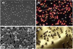
To fabricate the tunable absorber, silver nanocubes were synthesized by reducing silver nitrate with ethylene glycol in the presence of poly(vinyl pyrrolidone) (PVP). The molar ratio of PVP relative to silver nitrate determines the geometric shape and size of the resultant nanocubes (see figure). Next, the fabricated silver nanocubes are adsorbed on a thin polymer layer over the gold film using colloidal self-assembly processes.
Although 3% coverage of 74 nm (on a side) ideal cube-shaped nanocubes enables greater than 93% absorption over an approximate 40-nm-wide wavelength region that is tunable across the visible spectrum from approximately 500–800 nm for a 50-nm-thick gold layer, less-than-ideal shaped nanocubes with slightly different sizes require increased coverage (up to 17.1% of the surface area). And as the polymer layer thickness is increased beyond the ideal 6 nm value, reflectance is increased.
“The most amazing aspect of these cubes is probably the many different things they can do,” says Antoine Moreau, assistant professor at Clermont University. “You could, for instance, turn your gold surface into a display screen by controlling the space between the cubes and the gold film to tune the color of the structure. But because the nanocubes are the tiniest interferometers we’ve ever seen, we first plan to use them to detect molecular changes in their environment or to explore the limits of our current electromagnetic description of metals. Ultimately, we hope to use this technology in the infrared to develop new thermophotovoltaic devices.”
REFERENCE
1. A. Moreau et al., Nature, 492, 7427, 86–89 (Dec. 6, 2012).

Gail Overton | Senior Editor (2004-2020)
Gail has more than 30 years of engineering, marketing, product management, and editorial experience in the photonics and optical communications industry. Before joining the staff at Laser Focus World in 2004, she held many product management and product marketing roles in the fiber-optics industry, most notably at Hughes (El Segundo, CA), GTE Labs (Waltham, MA), Corning (Corning, NY), Photon Kinetics (Beaverton, OR), and Newport Corporation (Irvine, CA). During her marketing career, Gail published articles in WDM Solutions and Sensors magazine and traveled internationally to conduct product and sales training. Gail received her BS degree in physics, with an emphasis in optics, from San Diego State University in San Diego, CA in May 1986.
