PHOTONIC CRYSTALS: Liquid crystal control improves with new self-assembly technique
Researchers from the University of Pennsylvania have demonstrated a new method to direct the assembly of photonic liquid crystals, generating small features that spontaneously arrange in arrays based on much larger templates.1Directed assembly is a growing field of research in nanotechnology and nanophotonics in which scientists and engineers aim to manufacture structures on the smallest scales without having to individually manipulate each component. They precisely define the starting conditions and let the physics and chemistry that govern those components do the rest.
The study was led by Shu Yang, associate professor in the School of Engineering and Applied Science’s departments of Materials Science and Engineering and Chemical and Biomolecular Engineering; Kathleen Stebe, Engineering’s vice dean for research and professor in Chemical and Biomolecular Engineering; and Randall Kamien, professor in the School of Arts and Sciences’ Department of Physics and Astronomy.
They came together through Penn’s Materials Research Science and Engineering Center, which recently received a $21.7 million National Science Foundation grant to support this kind of interdisciplinary research. Stebe and Kamien are leaders of the Center’s subgroup focused on elasticity in soft materials and knew they had the expertise on hand to do groundbreaking work with liquid crystals.
Location counts
If the location of liquid crystal defects can be controlled, the change in pattern or orientation can be put to use. In a liquid crystal display (LCD), for example, the crystals’ orientation in different regions determines which parts of the screen are illuminated. “Liquid crystals naturally produce a pattern of close-packed defects on their surfaces,” Yang said, “but it turns out that this pattern is often not that interesting for device applications. We want to arbitrarily manipulate that pattern on demand.”
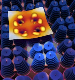
Electrical fields are often used to change the crystals’ orientation, as in the case with LCDs, but the Penn research team was interested in manipulating defects by using a physical template. Using a class of liquid crystals that forms stacks of layers spaced in nanometers—smectic liquid crystals—the researchers set out to show that, by altering the geometry of the molecules on the bottommost layer, they could produce changes in the defect patterns on the topmost (see figure). “The molecules can feel the geometry of the template, which creates a sort of elastic cue,” Stebe said. “That cue is transmitted layer by layer, and the whole system responds.”
The template was a series of microscopic posts arrayed like a bed of nails. By altering the size, shape, symmetry, and spacing of these posts, as well as the thickness of the liquid crystal film, the team can make subtle changes in the defect patterns.
A smectic liquid crystal that would naturally form a hexagonal array of dimple-like defects on its surface could be templated to form a square pattern or have dimples that were more closely or loosely packed. “The first layer’s molecules tend to be pinned to the edges of the posts,” Kamien said, “so changing a post’s size and shape will change how many defects can sit on its edges at the same time.”
Beyond sensors and displays, these defects can be used in nanomanufacturing. “If you make defects like dimples, you could put ink in them and use them like a stamp,” Kamien said. “Or you could make the inverse of the dimples and make points, which could be used as localized surface plasmon resonance hot spots for chemical and biological sensing or as a topographic protrusion for creating a superhydrophobic surface.”
Because the layers of liquid crystals transmit elastic energy, they can also be used to do mechanical work. The top layer could be used as a template to assemble even larger molecules. By establishing the mathematical relationships between the post parameters and the surface-layer defects, the researchers are laying the foundation of a directed assembly technique that can be used with any smectic liquid crystal.
REFERENCE
1. A. Honglawan et al., Proc. Nat. Acad. Sci., 110, 1, 34–39 (2013); doi:10.1073/pnas.1214708109.

Gail Overton | Senior Editor (2004-2020)
Gail has more than 30 years of engineering, marketing, product management, and editorial experience in the photonics and optical communications industry. Before joining the staff at Laser Focus World in 2004, she held many product management and product marketing roles in the fiber-optics industry, most notably at Hughes (El Segundo, CA), GTE Labs (Waltham, MA), Corning (Corning, NY), Photon Kinetics (Beaverton, OR), and Newport Corporation (Irvine, CA). During her marketing career, Gail published articles in WDM Solutions and Sensors magazine and traveled internationally to conduct product and sales training. Gail received her BS degree in physics, with an emphasis in optics, from San Diego State University in San Diego, CA in May 1986.
