PHASED ARRAYS: Nanophotonic array is CMOS-compatible
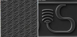
Using silicon fabrication technology, a team at the Massachusetts Institute of Technology (MIT; Cambridge, MA) has taken a huge leap forward in the development of phased arrays of optical nanoantennas by creating a passive 64 × 64-element array on a millimeter-sized silicon chip.1 The resulting device projected fixed images of the MIT logo. The researchers also made a smaller 8 × 8 array that can be phase-modulated to steer the beam. The largest previous optical phased arrays were only 4 × 4 elements.2
The devices are optical analogs of radio-frequency phased-array antennas, used to generate highly directional and steerable radio emission. The array size and spacing depends on wavelength, so radio-frequency arrays are large; optical arrays must be proportionately smaller, posing a different set of challenges.
Although it’s relatively easy to squeeze many tiny emitting elements into a small area, the optical couplers and phase shifters needed to control them “tend to be tens or hundreds of wavelengths long, which requires a large distance between each antenna,” wrote Thomas Krauss of the University of York (York, England) in a commentary in the journal Nature.3 As a result, optical phased arrays had been limited to no more than 16 elements.
CMOS fabrication
Michael Watts and colleagues at MIT overcame those limits by turning to a fundamentally new architecture compatible with complementary metal-oxide semiconductor (CMOS) fabrication. The passive array is a planar silicon structure fabricated on the top of the CMOS oxide layer. An optical fiber delivers light from an external 1.55-μm-emitting infrared (IR) laser to a network of silicon waveguides on the chip surface (see figure). The light enters one waveguide that runs along the side of the array, evanescently coupling into a series of 64 branches, with the coupling length increasing gradually along the light path so that each branch receives an equal input power. Each branch waveguide, in turn, evanescently couples to a series of 64 unit cells, with coupling length adjusted in the same way so that all 4096 cells receive the same input power.
Each unit cell is 9 μm2 and includes an optical-delay line delivering light from the branch waveguide to the antenna. Lengths of the delay lines differ by a few nanometers between adjacent cells and up to a full wavelength across the 64 antenna cells. The antenna structure is a series of planar silicon arcs designed to radiate most of the light upward from the chip, although not normal to the surface to avoid backreflection.
“The amazing thing was that we were able to line up all those phases statically in fabrication, and all 4000 elements phased up automatically,” Watts says. Within an hour, the researchers had located the far-field image and observed the IR pattern of MIT logos.
Thermo-optic phase-shifting
The next step was to make a smaller 8 × 8 array with tunable phase delays so the antenna output could be moved. They used the same basic architecture but added silicon electrical connections to the silicon waveguide. Passing a modest current through the optical delay line heats it, causing a thermo-optic phase shift; thermal isolation limits heat transfer. Tuning the phase shifts of the antennas dynamically steered and shaped the emitted light. Applying different voltages to the antenna elements produced five different patterns that agreed with computer predictions. A video posted along with the team’s Nature paper demonstrates both beam steering and splitting beams into two or four images.
The static optical array, which was easier to make, showed that the concept could be scaled to large arrays. But, Watts says, “The active one is what we’re after. You can use it to project arbitrary patterns.” They started small to keep wiring requirements simple. Larger dynamic arrays would require so many connections coming from behind them that it would be simpler to fabricate CMOS circuits behind the nanophotonic antennas. “We are going to a fully active version with CMOS behind it,” says Watts, who hopes to complete such a version within several months.
Near-term goals include beam steering for lidar and free-space communications. A chip-based lidar could be installed in cars for collision avoidance. The Nature paper acknowledges funding from DARPA’s SWEEPER program, which lists as one goal an 8 × 8 beam-steering array.
Use in biomedical imaging is another goal. A beam-steering chip could be put on the end of an optical fiber for optical coherence tomography (OCT) during endoscopy or perhaps intravascularly. The image of the MIT logo looked flat, but Watts says, “It’s truly holographic, and we could have made it three-dimensional.”
So far the researchers have only modulated phase, but in principle they also could add an electro-absorption modulator or Mach-Zehnder interferometer to control amplitude. Both are needed for high-quality 3D holography. Another possibility, Krauss suggests, is imaging through turbid media, using a phased array as an adaptive optical element to compensate for scattering.
The first experiments used near-IR lasers because silicon is transparent in that range. Optical phased-array antennas for visible light would require a different material: Watts would use silicon nitride to reach the visible. “It would require changing a lot of things,” he says, but it offers the high refractive-index contrast needed for steerable arrays.
REFERENCES
1. J. Sun et al., Nature (Jan. 10, 2013); doi:10.1038/nature11727.
2. K. Van Acoleyen et al., Opt. Exp., 18, 13655 (June 21, 2010).
3. T.F. Krauss, Nature, 493, 170 (Jan. 10, 2013).

Jeff Hecht | Contributing Editor
Jeff Hecht is a regular contributing editor to Laser Focus World and has been covering the laser industry for 35 years. A prolific book author, Jeff's published works include “Understanding Fiber Optics,” “Understanding Lasers,” “The Laser Guidebook,” and “Beam Weapons: The Next Arms Race.” He also has written books on the histories of lasers and fiber optics, including “City of Light: The Story of Fiber Optics,” and “Beam: The Race to Make the Laser.” Find out more at jeffhecht.com.
