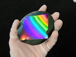
Nanoimprint diffraction gratings improve solar-cell efficiency
Because crystalline silicon (c-Si) solar-cell manufacturers are using thinner wafers to reduce costs, solar light-trapping technologies are becoming increasingly important. Researchers from the Fraunhofer Institute for Solar Energy Systems (ISE; Freiburg, Germany) and Universidad Politécnicat de Madrid (Madrid, Spain) are using rear-side diffraction gratings to capture photons—especially near the c-Si band edge (1.2 μm wavelengths)—that are lost as wafer thickness decreases. The gratings deflect the photons within the cell where they are contained through total internal reflection and have longer path lengths to increase absorption chances.
The researchers used two different dielectric buffer layer (DBL) processes and a low-cost aluminum backreflector in a nanoimprint-lithography process to fabricate the gratings. The DBLs were designed specifically to prevent absorption by the rear-reflector mirror—a problem that sometimes occurs with grating-based light-trapping designs. Binary gratings with a 50% duty cycle and 1 μm period were predicted to be optimum for photon absorption in 40-μm-thick c-Si substrates. Solar-cell efficiency was found to be enhanced between 0.8% and 1.3% using the rear-side gratings. Contact Alexander Mellor at [email protected].

Gail Overton | Senior Editor (2004-2020)
Gail has more than 30 years of engineering, marketing, product management, and editorial experience in the photonics and optical communications industry. Before joining the staff at Laser Focus World in 2004, she held many product management and product marketing roles in the fiber-optics industry, most notably at Hughes (El Segundo, CA), GTE Labs (Waltham, MA), Corning (Corning, NY), Photon Kinetics (Beaverton, OR), and Newport Corporation (Irvine, CA). During her marketing career, Gail published articles in WDM Solutions and Sensors magazine and traveled internationally to conduct product and sales training. Gail received her BS degree in physics, with an emphasis in optics, from San Diego State University in San Diego, CA in May 1986.
