SPECTROMETERS: Miniature spectrometer designs open new applications potential
Driven by developments in spectrograph optical components, array detectors, fiber-optics, and computing, a significant reduction in the size of optical spectrometers has been realized without sacrificing performance. This has resulted in the commercialization of a new class of low-cost, compact spectrometers, commonly referred to as miniature spectrometers. Viewed as novelty devices when first developed almost 20 years ago, they are now used for applications that were previously carried out by larger, more sophisticated bench-mounted versions. However, limitations in spectral manipulation, data transfer speed, and multichannel measurement capabilities have limited their use for more demanding application areas.
This article will introduce the fundamental principles of miniature spectrometers and describe a "smart" design that includes an embedded microprocessor to improve signal-to-noise ratio (SNR), a significant enhancement in the speed of transferring data, and the simultaneous synchronization of up to 32 channels of data.
Basic principles
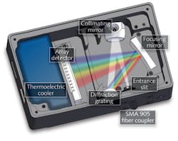
The basic function of a miniature spectrometer is to take light, break it into spectral components, digitize the signal as a function of wavelength, and read it out and display it through a computer.1 The first step in this process is to direct light through a fiber-optic cable into the spectrometer through the entrance slit. The light is then collimated by a concave mirror and directed onto a grating. The grating disperses the spectral components of the light at slightly varying angles, which are then focused by a second concave mirror and imaged onto the detector array (see Fig. 1).
Once imaged, the photons are converted into electrons that are digitized and read out through a USB or serial port to an external computer. Software interpolates the signal based on the number of pixels in the detector and the linear dispersion of the diffraction grating to create a calibration that enables the data to be plotted as a function of wavelength over the given spectral range. These data can then be used and manipulated for many different spectroscopic applications.
Optical components used in miniature spectrometers—such as slits and gratings—are usually optimized depending on the intended application requirements. However, there are three critical areas in a spectrometer's design that have an impact on whether it can be used for more demanding work: spectrograph design, detector technology, and data processing.
Spectrograph design
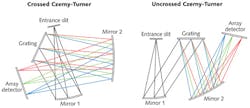
The Czerny-Turner optical configuration is recognized as the most suitable for miniature spectrometers because of its compact design, typically consisting of two concave mirrors and one flat diffraction grating.2 The focal length of the first mirror is selected such that it collimates the light emitted from the entrance slit and directs it onto the diffraction grating. Once the light has been separated into its chromatic components, the second mirror is then used to focus the dispersed light from the grating onto the detector plane. Because of its crossover design, this configuration is known as a crossed Czerny-Turner optical bench.
The focal length of the two mirrors can be designed to provide various dispersion values, which in turn determines the spectral coverage and resolution of the system. By optimizing its geometry, the crossed Czerny-Turner spectrograph provides a flattened spectral field with very little distortion. However, because of its off-axis geometry, it exhibits quite large aberrations, which can significantly broaden the image width of the entrance slit. For that reason, the crossed Czerny-Turner optical bench is typically used for low-to-medium-resolution applications, employing parabolic mirrors to correct for spherical aberrations, when two-dimensional imaging is required.
To minimize these image aberrations, they are generally designed with a high f-number (>3), which in turn reduces its light throughput. The f-number of an optical system expresses the diameter of the optical image in terms of its effective focal length and is used to characterize the spectrometer's light gathering power. Unfortunately, the relatively high f-number of the crossed Czerny-Turner optical bench, when used with multimode fiber-optics, causes a fairly high level of stray light.
One simple and cost-effective way to resolve this issue is by uncrossing the optical bench. This allows for the insertion of "beam blocks" into the optical path, greatly reducing the stray light and, as a result, the optical noise of the system. This is not so much of a problem in the visible and near-infrared (NIR) regions where there is an abundance of signal and higher quantum efficiencies, but it can be a problem for dealing with low-light-level, ultraviolet (UV) applications. This makes the uncrossed (or traditional) Czerny-Turner spectrograph ideal for UV applications that require a compact form factor (see Fig. 2).Detector technology
While photodetectors can be characterized in many different ways, the most significant difference is in the detector material.3 Based on the bandgap energy, it's a general rule of thumb that the maximum theoretical wavelength of silicon-based detectors is 1117 nm. Indium gallium arsenide (InGaAs) detectors can be used between 840 and 3330 nm depending on the ratio of indium, gallium, and arsenic, but are typically used up to a maximum of 1700 nm.
The lower-wavelength-limit detection capability of a detector is slightly harder to quantify because it is determined by the absorbance characteristics of the semiconductor material used, and as a result can vary widely with the thickness of the detector. However, a common cost-effective method of improving the detection capability in the lower wavelength region is to place a fluorescent coating (typically phosphor-based) on the window of the detector to absorb the higher-energy photons and re-emit lower-energy photons, which are then detectable by the sensor.
Silicon multielement detectors are readily available in three different designs: conventional (front-illuminated) charge-coupled device (CCD), back-thinned CCD (BT-CCD), and photodiode array (PDA), while InGaAs detectors are generally only available in PDA configuration.
Conventional CCD detectors. CCDs can be constructed inexpensively, which makes them an ideal choice for most miniature spectrometers, but unfortunately they do have two limitations. First, the gate structure on the front of the CCD can cause the incident light to scatter and therefore not be absorbed. Second, in most commercial CCDs, the silicon (Si) surface is ion-implanted with phosphorus and this layer is kept relatively thick in order to facilitate low-cost production. This positively doped silicon (p-Si) substrate limits the efficiency of the detector (especially at shorter wavelengths) due to absorption effects through the p buried-channel layer.
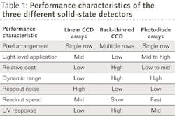
BT-CCD detectors. To alleviate the problems associated with conventional CCD technology and particularly where very high sensitivity is needed, BT-CCDs are the preferred choice. While there are distinct advantages to using BT-CCDs in spectroscopic applications, they have two major drawbacks. First, this process greatly increases the cost of production, and second, there can be problems caused from reflections off the front and back surfaces of the detector (etaloning effect) because the detector is so thin. This effect can be mitigated by processes such as deep depletion, but these add additional cost to the manufacturing process.PDA linear detectors. These detectors consist of a set of individual photodiodes that are arranged in a conventional linear fashion using complementary metal oxide semiconductor (CMOS) technology. Even though they use large pixels and exhibit lower sensitivity, they have several advantages over CCD and BT-CCD detectors. First, the lack of charge transfer eliminates the need for a gate structure on the front surface of the detector, and greatly increases the readout speed. The second advantage is that the well depth is about three orders of magnitude higher than a conventional CCD (due to their larger physical size), which results in a much wider dynamic range and linear response. These properties make PDAs ideal for applications in which it is necessary to detect small changes in large signals.Often, the choice of which detector to use is dictated by the application and the spectral range of interest. However, there is some overlap in these areas, so the choice often comes down to the specification of the detector (see Table 1).
Detector cooling. One of the major breakthroughs in the performance of solid-state detectors has been in the use of thermoelectric (TE) cooling devices. Often referred to as Peltier coolers, these devices have enabled significantly lower noise levels, allowing for longer signal integration and, as a result, lower detection limits.4 To better understand the advantages of TE cooling, it is important to have a basic understanding of noise associated with any type of photon detector. Theory tells us that the total noise of any detector is the square root of the sum of all the noise components. The four main sources of noise found in an array detector include readout noise, shot noise, dark noise, and fixed pattern noise.
Cooling an array detector with a built-in thermoelectric cooler (TEC) is an effective way to reduce dark current (noise), therefore enhancing the effective dynamic range and lowering the detection limit. Studies have shown that with silicon-based CCD array detectors, the dark current goes up by a factor of two when the temperature increases by approximately 5° to 7°C, and goes down by a factor of two when the temperature decreases by the same amount.
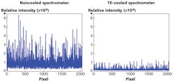
At room temperature (~22°C), for example, dark noise is a significant contribution to the total signal with a noncooled detector. Figure 3 shows the dark counts (noise) for a noncooled CCD spectrometer at room temperature and a TE-cooled spectrometer operating at 14°C using a 30 s integration time. The calculated root-mean-square (rms) noise level of the TE-cooled spectrometer on the right is approximately five-fold lower than the noncooled unit.Onboard data processing
A more recent development in the evolution of miniature spectrometers has seen the use of an embedded microprocessor onboard the spectrometer to carry out all the data manipulation, without having to send it to an external computer.5 Advantages of this approach include onboard data processing, which allows for rapid averaging, smoothing, and automatic dark current compensation to improve SNR; the USB 3.0 communication port, which provides a significant enhancement in the speed of transferring data; and ultrafast trigger delays, which enables simultaneous monitoring of multiple channels of data without the need to use a master/slave protocol.
To better understand the benefits this brings to spectroscopic studies, we will describe the design of the Exemplar miniature spectrometer. In addition to the normal scan mode used for traditional post-data manipulation using an external PC, a smart scan mode can carry out data processing within the spectrometer's onboard processor and a burst scan mode enables the internal spectral acquisition engine to send data back to the PC, with no time gap between the consecutive integrations, until the preset number of spectra is reached.
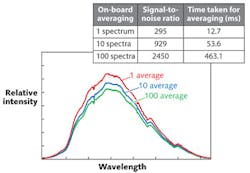
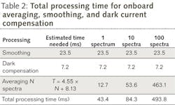
Smart scan. Smart scan allows for data manipulation to take place in the spectrometer's onboard processor, including averaging, smoothing, and dark compensation. When a smart-scan mode acquisition command is sent to the spectrometer, it will first perform the averaging, followed by the smoothing and dark compensation. After the data processing is finished, the spectrometer will send back a "handshake" to the PC to signal the readiness of the spectrum. The software will then send a "spectra retrieve" command to get the spectral intensity data corresponding to each of the individual physical detector pixels, or these data will remain stored in the spectrometer.A set of experiments were carried out by running up to 100 spectra over a fixed wavelength range of 350 to 1050 nm and calculating the SNR of each spectra and the time needed for each different method of data processing.6 These experiments are beyond the scope of this article, but three different sets of spectral data (average of 1, 10, and 100 spectra) using a measurement integration time of 1 ms show typical SNRs and the total time taken to carry out the averaging using the onboard processor (see Fig. 4). It can be seen that for 100 spectra to be accumulated, the total time taken is <0.5 s.Even when smoothing and dark compensation were carried out, total processing time to generate the spectral information was only slightly longer (see Table 2). If 1000 spectra were chosen, overall processing would take <5 s, significantly faster than sending the data to an external computer to be processed. In addition, all of the processing is done in parallel, so even if the number of channels is increased to 32, it will still only take <0.5 s to average 100 spectra or 5 s to average 1000.
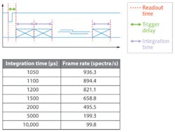
Burst scan. Burst scan is the fastest spectral acquisition mode available and takes advantage of the speed of transfer of the USB 3.0 communication port.7 After a burst-mode spectral acquisition command is received, the internal spectral acquisition engine will continuously send the data back to the PC until the preset number of spectra is reached. For optimal results, minimum integration time should be on the order of 1 ms because the two events of signal integration and spectral readout (plus sending the data to the external PC) are processed simultaneously.It is also important to emphasize that the trigger delay of this integration process is on the order of 14 ns ±1 ns jitter. This extremely fast external trigger mode allows for the synchronizing of up to 32 channels of data simultaneously, without the need to assign primary, secondary, or subsequent units or the use of additional hardware or circuitry.
Benefits of embedded processing
Miniature spectrometers have many advantages over traditional (benchtop) spectrometers because of their compact form factor and high sampling utility. As a result, they have been carrying out routine applications for the past 15 years, including transmission/reflection/absorption studies using UV, visible, and NIR spectroscopy, fluorescence spectroscopy, Raman spectroscopy, wavelength identification, and reflected color applications. They are also commonly used as components that are integrated into larger systems, such as microplate readers and thin-film measurement systems.
They have been restricted in scope and flexibility by limitations in computing and data transfer speed. The enhanced capability of spectrometers using embedded microprocessors has opened up the technology to applications that were previously beyond its capability. It remains to be seen what the practical benefits will be, but these will only be realized when they reach the real-world research community.
Some of the more demanding applications that could be addressed by this technology include:
Monitoring the kinetics of a chemical or biochemical reaction. This means measuring a distinctive change in the IR or UV absorbance transmission or fluorescence characteristics over time to understand when a reaction is complete or a new product has been formed. This is particularly applicable to molecular diagnostic testing, where hundreds of samples need to be rapidly tested in microplate readers to measure an expressed protein or organic molecule that confirms a disease, cancer, or a cell mutation.
Industrial process monitoring. Some of these techniques include online surface inspection, 3D imaging, and fiber-optic sensors, as well as spectroscopic and light-scattering process analyzers. The ability to monitor many process lines at the same time would benefit from the technology.
Simultaneous multichannel analysis. One example includes fast fiber-optic multichannel spectrometers for simultaneous measurements of visible and NIR absorption in the confirmation and measurement of defects in crystals. For this type of application, the speed of data capture over a spectral range of 400 to 1100 nm is critical for the basis in these kinds of experiments.
Time-of-flight (TOF) spectroscopy. Sampling all the incoming photons at exactly the same moment in time and transmitting them to the detector requires rapid, simultaneous measurement of the transmitted photons. This process could be addressed by the burst scan mode, as there is no gap between the two adjacent integration periods and spectral acquisition.
Multielement analysis using laser-induced breakdown spectroscopy (LIBS). Simultaneous detection capability is crucial because the emitted spectral wavelengths that correspond to the elemental fingerprint of a sample have to be detected and measured simultaneously. The ability to synchronously measure 12 channels of data would be advantageous for this measurement regime.
Spectroradiometric applications. Requirements for these include high-speed binning and sorting for the testing of visible illumination products such as LEDs, lighting, lamps, and bulbs. To that end, the much faster data transfer capability of spectrometers that use embedded microprocessors could be well suited to this process.REFERENCES
1. http://bwtek.com/spectrometer-introduction
2. http://bwtek.com/spectrometer-part-4-the-optical-bench
3. http://bwtek.com/spectrometer-part-3a-the-detector
4. http://bwtek.com/spectrometer-part-3b-the-detector
5. http://bwtek.com/technology/modular-solutions
6. B&W Tek Engineering Notes: Time needed for Smartscan (contact B&W Tek for a copy).
7. B&W Tek Engineering Notes: Frame rate >936 spectra/second (contact B&W Tek for a copy).

Robert V. Chimenti | Director, RVC Photonics LLC
Robert V. Chimenti is the Director of RVC Photonics LLC (Pitman, NJ), as well as a Visiting Assistant Professor in the Department of Physics and Astronomy at Rowan University (Glassboro, NJ). He has earned undergraduate degrees in physics, photonics, and business administration, as well as an M.S. in Electro-Optics from the University of Dayton. Over a nearly 20-year career in optics and photonics, he has primarily focused on the development of new laser and spectroscopy applications, with a heavy emphasis on vibrational spectroscopy. He is also very heavily involved in the Federation of Analytical Chemistry and Spectroscopy Societies (FACSS), where he has served for several years as the Workshops Chair for the annual SciX conference and will be taking over as General Chair for the 2021 SciX conference.
Robert J. Thomas | Principal Consultant, Scientific Writing Solutions
Robert J. Thomas is principal consultant at Scientific Writing Solutions. He has 12 years of experience as an analytical chemist; 20 years of experience working in product development, applications, sales, marketing, and customer training for a major scientific instrumentation company; and 10 years as a freelance science writer.
