PHOTONIC FRONTIERS: METAMATERIALS AND TRANSFORMATION OPTICS: Will transformation optics be the next optical revolution?

Metamaterials have changed the rules in optics. Nanostructured materials can manipulate light on a subwavelength scale, creating effects long considered impossible, from negative refraction to invisibility cloaks. In a dozen years, metamaterials have gone from a wild-eyed vision to one of the most exciting fields in photonics.
Yet the bright promise of metamaterials and the transformation optics based upon them has been slow to spread into practical applications. Invisibility cloaks can be demonstrated in the laboratory, but typically hide only small objects illuminated with monochromatic light and viewed at a specific angle. Key effects depend on resonances, so they don't work for broadband illumination. Nanostructures much smaller than optical wavelengths are hard to fabricate precisely, especially in volume. Structural materials with the desired interactions with light waves are hard to find. The challenges are to overcome these limitations and develop practical applications.
The growth of metamaterials
Metamaterials were demonstrated first at microwave frequencies, where they evolved from earlier studies of artificial dielectrics. The fundamental idea was to assemble arrays of many subwavelength components—including conductors as well as dielectrics—into bulk structures with otherwise unobtainable properties, particularly the refractive index.
In conventional optics, the refractive index n normally is defined as the ratio of the speed of light in a vacuum to that in the material. However, the underlying physics depend on two more fundamental quantities, the electrical permittivity ε and magnetic permeability μ, and n actually is equal to
n = ±εμ
Both ε and μ are defined as 1 in a vacuum, so n =1 for vacuum. Both quantities are positive in dielectrics such as glass, but conductors have negative permittivity and positive permeability at visible wavelengths, so their complex refractive index has a large negative component, and metals thus have a high attenuation.
Refractive index is uniform throughout natural materials of uniform composition, because the light waves "see" a bulk material rather than atoms. Likewise, light waves "see" a metamaterial as having a uniform refractive index because the many identical, uniformly-spaced elements are much smaller than the wavelength. However, the building blocks can be designed to have values of permeability and permittivity that give them refractive indexes impossible to achieve with conventional optics, such as n=-1, which bends light backward when it enters the metamaterial.
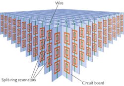
The effective permittivity and permeability of metamaterials depend on how the waves interact with internal elements. Regular arrays of metal wires, such as the ones shown in Fig. 1, can produce effective permittivity ranging from positive to negative, depending on size, spacing, and arrangement. Likewise, adjusting the design of split-ring elements like those shown in Fig. 2 can produce a wide range of permeability. The optical effects are analogous to those of radio waves with arrays of subwavelength antennas.Transformation optics
Metamaterials made up of uniform arrays of subwavelength elements are essentially customized materials designed to have unique properties. However, expanding designs to include non-uniform arrays of subwavelength elements greatly expands the options, opening the door to a field called transformation optics, which moves beyond ray optics to manipulate electromagnetic fields within the metamaterial.
"Our intuitive understanding of light has its foundations in the ray approximation, and is intimately connected with our vision. As far as our eyes are concerned, light behaves like a stream of particles," metamaterial pioneer John Pendry of Imperial College (London, England) wrote in Science.1 The standard ray approximation treats light as passing in straight lines through volumes with a uniform refractive index. However, the ray picture fails on the subwavelength scale where structures can be designed to alter the propagation of electric and magnetic field lines in arbitrary ways impossible with conventional bulk optics. That's the realm of transformation optics.
Conventional optics uses Fermat's principle to describe how the variation of refractive index affects light propagation along a path. "The emerging field of transformation optics enables us to solve the inverse problem; that is, how to realize a specific light path by designing the variation of material properties," write Yongmin Liu and Xiang Zhang.2 Thus, they can specify the path they want to guide light along in order to hide an object with an invisibility cloak, then use transformation optics to design the metamaterial needed to make the light follow that path.
Fig. 3 shows the light paths needed to design an invisibility cloak in two dimensions, which bend around the hidden object; transformation optics is used to design the metamaterial cloak. Transformation optics likewise can design the structural elements of metamaterials needed to produce various types of lenses, beam rotators, beam shifters, and optical illusions.Metamaterial building blocks
The fundamental building blocks of transformation optics are the same types of subwavelength elements as those used in other metamaterials. In addition to metals, they include dielectrics, and metal-dielectric structures that generate surface plasmon polaritons at their interface. The sizes and shapes of these elements vary through the metamaterial to produce the desired transformations. Individual elements must be smaller than the wavelength, 400 to 700 nm for visible light, or somewhat over a thousand atoms wide in a solid.
Researchers are exploring many options. Metals have a strong magnetic response useful in producing unusual interactions, but they suffer from high losses in the near-infrared and visible. Responses differ among metals in the optical and infrared bands. Resonant effects in metal structures can produce strong interactions, but the effects peak over a limited range. Dielectrics offer more broadband response and lower losses.
Among the possibilities being explored are nanocavity resonances in dielectrics with high refractive index, which offer lower losses than metals and are smaller than the vacuum wavelength because of their high index. For example, Lei Shi and colleagues at the Polytechnic Institute of Valencia (Madrid, Spain) have studied near-infrared resonances in silicon colloids as small as 250 nm, which they consider promising for metamaterials in both air and liquids such as water.3
Planar metasurfaces
Fabrication of bulk optical metamaterials has been challenging, so some researchers are studying planar structures. "Optical metasurfaces offer the fascinating possibility of controlling light with surface-confined, flat components," Vladimir Shalaev and colleagues at Purdue University (Bloomington, IN) recently wrote. "Metasurfaces enable new physics and phenomena that are distinctly different from those observed in their 3D counterparts."4 They also are compatible with on-chip nanophotonics.
Their metasurfaces are thin patterns of metal and dielectric deposited on a substrate. Their response deviates from bulk reflection and refraction, and depends on optical dispersion in the subwavelength layer. So far, demonstrations have included surface antenna arrays for negative refraction at infrared wavelengths, as shown in Fig. 4, and planar chiral effects at optical wavelengths. Metasurfaces also have produced 3D effects without the use of bulk materials, and the Purdue group hopes that they also can control optical phase, polarization, and frequency.Phase-change materials could be integrated into planar semiconductor metasurfaces for applications such as optical switching, beam steering, pulse shaping, or modulation, the Purdue group writes. They also suggest the possibility of making hyperbolic metasurfaces, analogous to the bulk hyperbolic metamaterials made by alternating metal and dielectric components to produce strong anisotropy and hyperbolic dispersion. Bulk versions can dramatically change the behavior of light, but are lossy and hard to make. However, the Purdue group says quasi-two-dimensional hyperbolic metasurfaces would have lower loss and could be used with standard semiconductor technology.
Outlook
Transformation optics has become a powerful paradigm for exploiting the potential of optical metamaterials. "Physical insight is the key benefit of this approach to electromagnetism," wrote Pendry, predicting "transformation optics will be the design tool of choice in electromagnetic theory."
The challenges may be as large as the promise. The metamaterials revolution is going in many directions at once in laboratories around the world. New breakthroughs are needed in design and fabrication of nanostructures. There's no agreement on the best shapes and materials for assembling metamaterials. Applications remain uncertain. Like the laser half a century ago, metamaterials today seem like a solution in search of a problem—but we know how that one worked out.
REFERENCES
1. J. B. Pendry et al., Science, 337, 549 (2012); doi:10.1126/science.1220600.
2. Y. Liu and X. Zhang, Nanoscale, 4, 5277 (2012); doi:10.1039/c2nr31140b.
3. L. Shi et al., Adv. Mat., 24, 5934–5938 (2012); doi:10.1002/adma.201201987.
4. A. V. Kildishev et al., Science, 339 (2013); doi:10.1126/science.1232009.

Jeff Hecht | Contributing Editor
Jeff Hecht is a regular contributing editor to Laser Focus World and has been covering the laser industry for 35 years. A prolific book author, Jeff's published works include “Understanding Fiber Optics,” “Understanding Lasers,” “The Laser Guidebook,” and “Beam Weapons: The Next Arms Race.” He also has written books on the histories of lasers and fiber optics, including “City of Light: The Story of Fiber Optics,” and “Beam: The Race to Make the Laser.” Find out more at jeffhecht.com.


