ACOUSTO-OPTICS: Colored picosecond acoustics extend to thin-film characterization
Bulk acoustic-wave (BAW) resonators—used in optical networks, radio-frequency instrumentation, sensors, and radar systems (typically at frequencies above 2 GHz)—consist of thin-film layers of piezoelectric and semiconductor materials sandwiched between metal electrodes. In 2006, femtosecond lasers were shown to be capable of generating and detecting very high frequency acoustic waves that could characterize the thickness and material properties of the various BAW layers.1 Today, a modified and improved wavelength-specific picosecond acoustic technology called colored picosecond acoustics (APiC) developed by CEA-Leti (Grenoble, France) and Menapic (Lille, France) not only measures microns-thick bulk layered devices, but also characterizes nanometer-scale thin-films.2
Picosecond acoustics
In the APiC experimental setup, an initial pump pulse is incident at the surface of a sample where it is absorbed. This pump pulse generates an acoustic-strain pulse that is related to absorption (which is very high for metals). Only longitudinal waves are excited by the pump pulse, because the strain length is a tiny fraction of the few-tens-of-microns diameter of the pump-pulse beam.
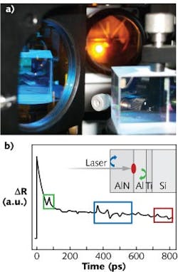
The strain pulse propagates in the film at the longitudinal sound velocity of a few nanometers per picosecond. As the strain pulses reflect from the various film layers in the stack, the echoes return to the surface of the material and modify the dielectric constant of the film. A second probe-laser pulse detects these changes, as reflection or transmission is affected by the acoustic strain wave itself. By adjusting the pump-probe delay, the echoes can be analyzed to determine layer thicknesses.
For the pump-probe source, a Ti:sapphire tunable laser produces 120 fs optical pulses at a 76 MHz repetition rate at wavelengths between 700 and 990 nm. The beam is split to provide pump and probe signals at crossed polarizations. With pump and probe pulses centered at 780 nm, the thickness of a BAW with a 2 μm layer of aluminum nitride (AlN) followed by a 200-nm-thick Al film and a 50-nm-thick titanium (Ti) film were easily measured with an accuracy of about 6% (see figure).
Because coupling between the acoustic-strain pulse and the probe beam is very sensitive to wavelength, using a blue-wavelength probe pulse can refine the measurement to determine both layer thickness and sound velocity, as well as enable a thickness accuracy of approximately 0.2%.
Higher sensitivity for thinner films
To characterize nanometer-scale thin films such as diamond, Menapic refined the APiC measurement setup. Using an 840 nm pump wavelength and multiple probe wavelengths, diamond films were characterized not only for physical dimensions, but for the elastic properties of nanocrystalline and polycrystalline type films. The measurement can be applied to films with thicknesses down to a few tens of nanometers.
“The discovery developments for nanoelectronic concepts and devices are increasingly based on the knowledge of material properties through modeling steps. Indeed, regarding the equipment investments required to push forward micro- and nanodevices development, modeling is cost-effective,” says Menapic president Patrick Emery. “Due to the size of the constitutive elements of nanoelectronics devices, the understanding of multiphysics coupling and failure mechanisms challenges the current characterization capabilities. Combined with its micron-sale measurement spot size, the sensitivity of APiC offers a way to perform measurements of elastic properties with improved lateral and depth resolutions.”
REFERENCES
1. A. Devos et al., Proc. 2006 IEEE Ultrasonic Symposium, paper 4F-5 (2006).
2. http://bit.ly/10qRDA2.

Gail Overton | Senior Editor (2004-2020)
Gail has more than 30 years of engineering, marketing, product management, and editorial experience in the photonics and optical communications industry. Before joining the staff at Laser Focus World in 2004, she held many product management and product marketing roles in the fiber-optics industry, most notably at Hughes (El Segundo, CA), GTE Labs (Waltham, MA), Corning (Corning, NY), Photon Kinetics (Beaverton, OR), and Newport Corporation (Irvine, CA). During her marketing career, Gail published articles in WDM Solutions and Sensors magazine and traveled internationally to conduct product and sales training. Gail received her BS degree in physics, with an emphasis in optics, from San Diego State University in San Diego, CA in May 1986.
