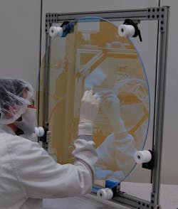
In addition to its ion-beam-sputtering (IBS) deposition process that can uniformly coat half-meter optics, MLD Technologies has scaled up its atomic-layer-deposition (ALD) process to provide uniform (less than ±1% variation), low-loss (typically less than 50 ppm total loss) precision optical coatings on substrates up to 800 mm in diameter.
The ALD process creates pinhole-free coatings one monolayer at a time from the chemical reaction of gas-phase precursors for excellent barrier properties for wet or corrosive chemical environments. Coating designs for the near-ultraviolet to mid-infrared wavelength region can be deposited from a number of metal-oxide film materials. The production-scale ALD chamber designed and built by MLD is capable of coating planar, 3D, and large curved optical elements. A pilot-scale chamber is also available to coat substrates smaller than 250 mm diameter and for process development. MLD can also produce hybrid coatings, comprised of IBS layers in combination with ALD layers. These hybrid coatings are critical, for example, when fabricating high-energy laser mirrors or other optics exposed to harsh chemical or corrosive environments. Contact Ric Shimshock at [email protected].
About the Author

Gail Overton
Senior Editor (2004-2020)
Gail has more than 30 years of engineering, marketing, product management, and editorial experience in the photonics and optical communications industry. Before joining the staff at Laser Focus World in 2004, she held many product management and product marketing roles in the fiber-optics industry, most notably at Hughes (El Segundo, CA), GTE Labs (Waltham, MA), Corning (Corning, NY), Photon Kinetics (Beaverton, OR), and Newport Corporation (Irvine, CA). During her marketing career, Gail published articles in WDM Solutions and Sensors magazine and traveled internationally to conduct product and sales training. Gail received her BS degree in physics, with an emphasis in optics, from San Diego State University in San Diego, CA in May 1986.
