EUV LITHOGRAPHY: High-NA EUV optics are on their way

By taking advantage of techniques such as 193 nm water-immersion optics, semiconductor photolithography has enabled shrinking of feature sizes on computer chips to around 22 nm. But wiggle room for traditional glass-based transmissive lithographic optics has shrunk; moving below 20 nm or so will require shorter wavelengths. With the development of 13.5 nm extreme-ultraviolet (EUV) light sources by Cymer (San Diego, CA) and others, as well as optics such as the NXE:3300 platform by ASML (Veldhoven, The Netherlands) with a numerical aperture (NA) of 0.33, EUV appears to be progressing toward practical use.
But—as with any optical system—the higher the NA, the better the potential resolution. As a result, SEMATECH (SEmiconductor MAnufacturing TECHnology Association) and the College of Nanoscale Science and Engineering at the State University of New York (both in Albany, NY), have a program to develop small-field EUV exposure tools with NAs of 0.5.
Recently, a team of researchers from Zygo Corporation’s Extreme Precision Optics (EPO) division (Richmond, CA), SEMATECH, Lawrence Berkeley National Laboratory (LBNL; Berkeley, CA), Hyperion Development (San Ramon, CA), and Lawrence Livermore National Laboratory (LLNL) and Spiller X-ray Optics (both in Livermore, CA) presented results of their efforts to produce and make a 0.5 NA EUV optical projection module.1
Modified Schwarzschild design
The design of the 5X-reduction projection optics, which are made of a material with a near-zero coefficient of thermal expansion, is based on a Schwarzschild design modified so that the mirrors are 16th-order aspheres with separated centers of curvature, as opposed to the standard Schwarzschild configuration with two concentric spheres. The field is small (20 × 300 μm) but is sufficient for research into EUV photoresists, photomask materials, and so on; the feature-size (half-pitch) resolution is 11 nm, and with certain illumination approaches such as extreme dipole illumination, can be as good as 8 nm. In addition, the optical system size (as well as the reduction ratio, mass, and other parameters) is constrained by a requirement that it fit into an existing research tool as an upgrade to the previous optics.
To achieve these results, the transmitted wavefront error of the two-mirror optical projection module is specified to be less than a 1 nm root-mean-square (RMS) over the entire image field. Zygo Corporation, which has two decades of experience in fabricating EUV optics and has previously supplied optics for EUV systems, is responsible for the modified-Schwarzschild mirror fabrication and metrology.
The large amount of asphericity in the new EUV mirrors leads to higher-frequency spatial periods than in previous designs, making polishing more difficult and necessitating more steps in the fabrication process. When added to the tight surface tolerances, fabricators and metrologists have their work cut out for them.
Fabrication and metrology
Zygo uses a high-precision five-axis milling machine with ultrasonic capabilities that boosted the material removal rate by a factor of up to four while reducing subsurface damage. The milling machine’s series of diamond tools lead to a ready-to-polish surface. Polishing is done using a subaperture computer-controlled optical surfacing technology developed at Zygo EPO, along with ion-beam figuring.
Monitoring of the process is done with coordinate-measuring machines, profilers, and interferometers; in a vertical cavity test, the interferometer uses a Zygo-fabricated computer-generated hologram as a diffractive null element in a vertical cavity test that imitates the as-used orientation of the mirror optics.
Minimizing both mid-spatial frequencies and microroughness is extremely important at EUV wavelengths. Zygo EPO designed a “sub-aperture surface height interferometric measuring instrument” (SASHIMI) with custom optics to match the tested asphere mirrors; the white-light instrument generates hundreds of subapertures that were then stitched together by software. Roughness at even higher spatial frequencies between 10 μm and 10 nm is characterized by an atomic-force microscope.
The period of the multilayer high-reflection coatings deposited on the mirrors is varied across the clear apertures to maximize reflectivity at the local angles of incidence; the molybdenum/silicon coating was developed at LLNL and is deposited using magnetron sputtering.
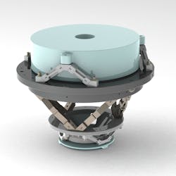
The optomechanical structure for the two mirrors is made from Super-Invar, which has a low CTE. The mirrors are mounted via bipod structures with integrated flexures (see figure); the relative orientation of and distance between the two mirrors are controlled using an actuator-driven hexapod structure.
Alignment of the optics and wavefront measurement is done via interferometer at a 633 nm wavelength to 0.5 nm RMS at the center of the field and 1.0 nm RMS at the edge of the field. Displacement sensitivities for the testing are high: for example, a 13 nm image-plane displacement produces 0.5 nm RMS of defocus error (which is easily tweaked out, but gives an idea of the other alignment sensitivities).
Performance of the system was computer-modeled; analysis included printing of 12 nm lines and spaces using annular illumination with a pupil fill of 0.93 and a donut-hole size of 0.36 of the pupil. Results showed an acceptable critical-dimension variation of ±10%. A simulation of printing 8 nm lines and spaces with extreme dipole illumination showed a depth of focus greater than 100 nm for a ±10% change.
The annular illumination configuration will be available on systems being created for the Albany and LBNL sites, while the extreme-dipole configuration is intended for the LBNL system.
REFERENCE
1. H. Glatzel et al., Proc. SPIE Advanced Lithography, 8679-42 (2013).
About the Author
John Wallace
Senior Technical Editor (1998-2022)
John Wallace was with Laser Focus World for nearly 25 years, retiring in late June 2022. He obtained a bachelor's degree in mechanical engineering and physics at Rutgers University and a master's in optical engineering at the University of Rochester. Before becoming an editor, John worked as an engineer at RCA, Exxon, Eastman Kodak, and GCA Corporation.
