Ge/Si near-IR CMOS-compatible photodetector has 1 A/W responsivity
One approach for creating efficient near-IR photodetectors in silicon photonics is germanium/silicon (Ge/Si) hybridization, where Ge detectors are bonded or grown on silicon photonic/electronic chips. But the lattice mismatch (difference in crystalline-lattice atomic spacing) between Si and Ge is about 4.2%, which produces many misfit dislocations that lead to high leakage current and mediocre responsivity. Now, researchers from Tyndall National Institute and University College Cork (both in Cork, Ireland) have developed an asymmetrically doped wafer-bonded Ge/Si heterojunction photodiode that has a very high responsivity greater than 1 A/W for a 1.55 μm wavelength.
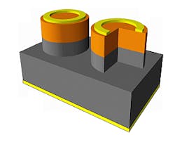
The p--Ge/n+-Si configuration was chosen to enable collection of electrons into the Si as a result of the more-favorable band offset. First, the Ge and Si were bonded under an air pressure of 10-5 mbar; after annealing, the Ge layer was mechanically thinned to 5.4 μm. Mesa-type diodes were fabricated, with titanium/silver ring electrodes created on the Ge mesas. In operation, both temperature and light level influence the band structure at the Ge interface, with holes accumulating at room temperature. These accumulated holes change the potential barrier height, boosting the dark current and thus the responsivity. The detector’s compatibility with CMOS processing makes it ideal for high-performance near-IR imaging devices with Si readout circuits. Contact Farzan Gity at [email protected].
About the Author
John Wallace
Senior Technical Editor (1998-2022)
John Wallace was with Laser Focus World for nearly 25 years, retiring in late June 2022. He obtained a bachelor's degree in mechanical engineering and physics at Rutgers University and a master's in optical engineering at the University of Rochester. Before becoming an editor, John worked as an engineer at RCA, Exxon, Eastman Kodak, and GCA Corporation.

