Numerous imaging applications cannot rely on ambient light and require artificial illumination. In cases where the illumination system should not be distracting, the illumination source should emit infrared (IR) light beyond 815 nm, where eye sensitivity is extremely reduced. But because silicon-based sensors with a 900 nm upper detection limit are cheaper than other types of sensors, light emission at 850 nm is a good match to achieve low-distraction illumination and low-cost detection systems. Oclaro’s high-power 850 nm vertical-cavity surface-emitting laser (VCSEL) arrays suit numerous IR illumination applications—including gesture-recognition technology and proximity sensing—and improve on legacy high-power IR light-emitting diodes (LEDs) and edge-emitting lasers.
Advantages of VCSELs
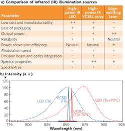
Both IR lasers (VCSELs and edge-emitting lasers, or EELs) and LEDs in the nonvisible 830–860 nm range can be manufactured using gallium arsenide (GaAs) materials. But numerous illumination criteria including cost, manufacturability, ease of integration, reliability and efficiency, modulation speed, and spectral parameters need to be considered (see figure).
Like LEDs, VCSELs emit light perpendicular to the substrate material. However, VCSEL emission is coherent, more directional, and spectrally defined. For an individual 850 nm multimode VCSEL, 23 mW of continuous-wave (CW) power is achievable. To achieve a larger emission area and higher power, 2D arrays of VCSELs can be connected in parallel. A 0.25 mm2 VCSEL array can emit more than 1 W of power in pulsed mode and more than 600 mW in CW mode; 3 W is possible in pulsed mode from a 0.45 mm2 array, but the array size can be increased to achieve tens or even hundreds of watts.
The VCSEL emission spectrum is defined by the cavity mode rather than by the optical gain, as with LEDs. For example, the typical full-width-at-half-maximum (FWHM) emission-wavelength bandwidth of an LED is around 30 nm and around 2 nm for a multimode VCSEL. In practice, for applications such as time-of-flight imaging where ambient light needs to be filtered out, narrower-band filters can be used in combination with VCSELs to improve signal-to-noise ratio of the system through better rejection of parasitic light. In addition, spectral shift with temperature is also defined by the VCSEL’s change of cavity mode (0.06 nm/°C) rather than by the change of the optical gain peak with temperature (0.3 nm/°C) for LEDs and EELs, enabling uncooled VCSEL-array sources.
The main limitation for LED modulation speed is related to the time it takes for carriers to recombine and generate light—a spontaneous emission-recombination process that occurs on a several-tens-of-nanoseconds timeframe, limiting modulation speeds to about 30 MHz. In contrast, the VCSEL recombination process is dominated by stimulated recombination that can be much faster: up to 25 Gbit/s modulation speeds for communication VCSELs. For a high-power VCSEL array, a rise time of 120 ps and fall time of 2 ns were measured using a 5 ns pulse and a low duty cycle (allowing overdrive), enabling output power of 5 W (>20 nJ) from an array otherwise designed to deliver 250 mW.
Because VCSEL emission consists of a narrow circular beam with an approximate 35° divergence angle, optics integration is simplified to allow smaller-form-factor modules than bulky LED-collimation architectures. Combined with a diffuser, a low-divergence VCSEL light source yields higher transmission efficiency and minimizes power consumption of the overall system through better photon usage.
“Arrays of VCSELs can be fabricated in any shape and tailored to match any pattern to any illumination shape—rectangular or even a linear light curtain,” says Julien Boucart, senior manager of product marketing for the industrial and consumer business at Oclaro. “Similar to LEDs and in contrast to EELs, the manufacturing process takes place at the wafer level, reducing manufacturing costs. And like LEDs, vertical emission means on-wafer testing and screening to further reduce costs and improve manufacturing quality and reliability. For our singlemode VCSEL line, for example, only one failure was observed out of about 90 million equivalent device hours for a reliability value better than 10 FITs [failures in time].”

Gail Overton | Senior Editor (2004-2020)
Gail has more than 30 years of engineering, marketing, product management, and editorial experience in the photonics and optical communications industry. Before joining the staff at Laser Focus World in 2004, she held many product management and product marketing roles in the fiber-optics industry, most notably at Hughes (El Segundo, CA), GTE Labs (Waltham, MA), Corning (Corning, NY), Photon Kinetics (Beaverton, OR), and Newport Corporation (Irvine, CA). During her marketing career, Gail published articles in WDM Solutions and Sensors magazine and traveled internationally to conduct product and sales training. Gail received her BS degree in physics, with an emphasis in optics, from San Diego State University in San Diego, CA in May 1986.
