LIGHT-EMITTING DIODES: GaN-on-GaN platform removes cost/performance tradeoffs in LED lighting
MIKE KRAMES
Despite high luminous efficacies and substantial potential savings in worldwide electricity consumption brought by the introduction of gallium nitride (GaN)-based white-emitting light-emitting diodes (LEDs) introduced in the 1990s, the present high prices and questionable light quality associated with these products threaten to limit adoption rates. The primary reason for the high cost of these white-light LEDs is the limited light-generating capability and complex semiconductor processing operations inherent to the use of foreign substrates as the materials platforms for most of today's GaN-based LEDs.
The new GaN-on-GaN platform from Soraa (Fremont, CA) enables unprecedented light output density and simplified LED architectures for high performance and lower overall cost. Regarding light quality, full-visible-spectrum LED technology made practical by the GaN-on-GaN platform eliminates the truncated spectra, poor color rendering capability, and fundamental illumination problems such as whiteness rendering associated with previous generation GaN-based LEDs based on primary blue emission.
Cost and performance
The transformation of general lighting to LED technology promises to have an enormous impact on worldwide electricity consumption for lighting (near 50% reduction by 2030) with corresponding reductions in carbon dioxide emissions.1 However, two major factors are slowing the adoption of energy saving LED technology for general lighting applications: cost and quality.
Unfortunately, the LED lighting industry risks repeating many of the same mistakes made by compact fluorescent lamp manufacturers such as prioritizing efficiency over quality and distracting customers with endless metrics rather than simply giving end-users what they want. Soraa's GaN-on-GaN technology addresses these two primary issues using a fundamentally different materials technology approach.
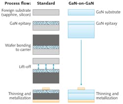
Materials science breakthroughs in Japan in the late 1980s and early 1990s enabled the first generation of GaN-based white-emitting (blue-pumped phosphor) LEDs that have dominated markets such as automotive, signage, and backlighting. These first-generation devices all involve depositing GaN epitaxial layers on some foreign substrate, such as sapphire (most common), silicon carbide, or silicon. Unfortunately, this heteroepitaxial approach to LEDs results in GaN-based active layers with poor crystalline characteristics (including defect densities of about 1,000,000 per square millimeter) and complicated semiconductor process flows and device designs. The resulting LEDs not only are expensive from a semiconductor manufacturing perspective, but also have limited power handling capability that places a ceiling on the potential lumen output and thus economic performance (lumens per dollar). The GaN-on-GaN approach side-steps these limitations by using a native GaN substrate developed for Blu-ray laser diodes for the active device layer deposition, resulting in 1000X lower defect density as well as a dramatically simplified wafer processing flow and lower bill of materials (see Fig. 1).
Native substrate advantages
In addition to the inherent atomic lattice matching for improved semiconductor crystalline quality and active region design, the native substrate provides several critical advantages with respect to performance: (1) high electrical and thermal conductivity for power leveling; (2) optical refractive-index matching for dispersing photons within the chip; and (3), volumetric design and shaping for increased surface area and higher light-extraction efficiency.
LEDs are inherently robust, but points of failure that do occur are usually driven by thermal gradients or "hot spots" that are generated by power density non-uniformities such as electrical current crowding. This is especially true in sapphire-based LEDs, because sapphire is electrically and thermally insulating (approximately 40 W/mK) and the relatively thin epitaxial layer stack (a few microns) has difficulty leveling power density across the chip at high drive currents. The same is true for thin-film LEDs wherein the substrate has been removed, limiting these LEDs in terms of their maximum drive current and subsequent light output. On the other hand, GaN-on-GaN LEDs enjoy very high electrical and thermal (approximately 230 W/mK) conductivities, can be driven at laser-diode-like current densities, and show no evidence of current crowding.2
Optical refractive-index matching is another advantage of the native substrate. In the case of sapphire-based LEDs, the low refractive index of approximately 1.77 compared to that of GaN at approximately 2.4 leads to significant light trapping within the device epitaxial layers and limits light-extraction efficiency. In the case of GaN-on-GaN, there is no reflection of light between the epitaxial layers and the substrate, and light propagates away from the absorbing areas of the device (active layer and electrodes) towards the chip outer surfaces from which it can be extracted as useful light.
This light-extraction effect underlines the importance of volumetric LED design for GaN-on-GaN since the substrate plays a pivotal role in overall light extraction—an option not available to sapphire-based or thin-film LEDs. Our GaN-on-GaN devices use thick side walls and a triangular shape to maximize light extraction, which is estimated at around 90% compared to the low 80 percentile for the best thin-film LEDs.3
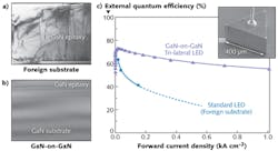
These advantages allow GaN-on-GaN LEDs to operate at unprecedented power densities while maintaining high efficiency. Typical performance of a violet-emitting GaN-on-GaN LED compared to a standard LED based on foreign substrates (using a data sheet with typical performance for a blue-emitting LED from a top tier supplier) shows that high external quantum efficiencies for the GaN-on-GaN LED are maintained up to current densities familiar to laser diodes (kA cm-2 regime). Meanwhile, the standard LED efficiency is limited and drops dramatically due to issues with current crowding and non-radiative processes related to crystalline defects and Auger recombination (see Fig. 2).4,5Since the primary objective of lighting manufacturers is not to ship wafers, but to ship lumens, the high light density of GaN-on-GaN provides the potential for enormous cost savings; in fact, higher current density means that one lot of GaN-on-GaN wafers is equivalent to about five to 10 lots of standard LED wafers. Combined with simplified fabrication steps and very high yields supported by very small chip sizes (400 µm triangular shape), the entitlement for overall cost per lumen for GaN-on-GaN is fundamentally and significantly lower than that of first-generation (foreign-substrate-based) GaN LEDs. Even today, at a relatively low state of maturity, GaN-on-GaN enables lighting products like Soraa's MR16 retrofit lamps with a cost-per-lumen value comparable to the best commercially available standard LED-based lamps.
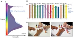
In addition, the higher power handling capability of GaN-on-GaN enables the development of LEDs based on higher (photon) energy violet emission, enabling efficient full-visible-spectrum LED lighting products for the first time. The penalty in energy (3.0 eV for violet compared to 2.7 eV for blue) is offset by the tremendous advantages in color quality with respect to illumination applications (see Fig. 3). In particular, the broad emission across all colors in the rainbow (violet to deep red) enables an excellent match to standard illuminants such as blackbody radiation (tungsten or tungsten-halogen incandescence) and unprecedented color rendering. For example, Soraa's VIVID MR16 lamp has a color rendering index (CRI) of 95 and a deep red (R9) color rendering of 95. Typical blue-based LEDs have a white emission spectrum that is truncated, are missing violet and deep red, and have a deficit in the cyan (approximately 500 nm) regime due to the fundamental Stokes gap between the LED primary blue emission and that of the phosphors it pumps.The violet-based GaN-on-GaN emission also provides photon energies sufficient to excite optical brightening agents (OBAs) in manufactured white materials like clothing, paper, plastics, and cosmetics.6 These OBAs have been developed over decades to make white materials look "white" when illuminated by conventional sources like daylight and incandescent bulbs. Standard blue-based LEDs cannot excite the OBAs, rendering white materials yellow and dingy in comparison to their targeted appearance under natural light. The combined effect of good color and whiteness rendering is striking (see Fig. 3).
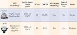
Advantages of GaN-on-GaN technology are best summarized in a comparison of specifications for Soraa's GaN-on-GaN VIVID MR16 lamp with the commonly used LED MR16 EnduraLED lamp from Philips (see table).7,8 Not only does the VIVID lamp outperform in intensity (center beam candlepower), color quality (CRI and R9), and whiteness rendering, but the inherent robustness of the underlying GaN-on-GaN LED technology also allows sealed-fixture use, single-beam operation, and a true Class 1 UL rating.Sealed, or enclosed, fixture operation is critical to allow retrofit LED MR16 lamps to be used in any existing lighting fixture, all of which were designed for halogen and many of which were not designed with air flow in mind. Retrofit lamp products that are not sealed-fixture compatible cannot be used in such fixtures and are not truly retrofit products.
Finally, single-beam operation is desirable to designers for directional lighting applications since it provides a single shadow rather than the "ghosting" effect caused by multi-LED "showerhead" lamps like the EnduraLED. The combination of these desired performance attributes is extremely difficult, if not impossible, for products based on foreign-substrate LEDs.
Soraa's GaN-on-GaN LED technology is in its early stages and the company expects not only further performance advantages, but also increased widespread deployment to other lighting products including larger directional lamps, downlights, non-directional lighting, and even new applications such as digital imaging and backlighting.
ACKNOWLEDGEMENT
GaN-on-GaN is a trademark of Soraa.
REFERENCES
1. U.S. Department of Energy, Solid-State Lighting Research and Development Multi-Year Program Plan, Office of Energy Efficiency and Renewable Energy, 1-84 (April 2013).
2. M. J. Cich et al., Appl. Phys. Lett., 101, 22, 223509 (2012).
3. A. David, IEEE J. Display Technol., 9, 5, 301-316 (2013).
4. Y-C Shen et al., Appl. Phys. Lett., 91, 14, 141101 (2007).
5. J. Iveland et al., Phys. Rev. Lett., 110, 17, 177406 (2013).
6. A. David et al., Opt. Exp., 21, 14, 16702-16715 (2013).
7. See http://bit.ly/1c4suRP.
8. See http://bit.ly/13BaE3h.
Mike Krames is CTO of Soraa, 6500 Kaiser Dr., Fremont, CA 94555; email: [email protected]; www.soraa.com.


