SiN CMOS-compatible integrated photonics aim at visible wavelengths
Silicon nitride (SiN) has a high refractive index compared to silicon dioxide (SiO2), which leads to tight confinement in SiO2-clad SiN waveguides; SiN is also compatible with standard complementary-metal-oxide semiconductor (CMOS) technology. These facts, and others, make SiN promising as a replacement for silicon in integrated photonics for some uses. Researchers at Aachen University (Aachen, Germany) and Illumina (Hayward, CA) have solved three problems that inhibited use of SiN for integrated photonics at visible
wavelengths.
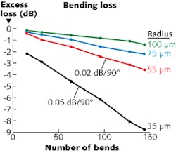
First, they created waveguides with an ultrathin (100 nm) film layer that boosts the interaction of the light field with the top cladding (important for sensing applications). Second, they created a free-space coupler for visible wavelengths (660 nm in the prototype) with an insertion efficiency in the range 38% to 44%. Third, they developed a multimode interference coupler (MMI) for splitting light within the circuit; the 57.3-μm-long MMI split one beam into four with an efficiency higher than 93% and an imbalance less than 10%. Waveguide losses were below 0.71 dB/cm and 0.51 dB/cm with water cladding and SiO2 cladding, respectively, and bend losses for various radii were low—for example, 0.02 dB per 90° bend for a 55 μm radius. Potential uses include biosensing in the visible and near-IR regions. Contact Sebastian Romero-García at[email protected].

John Wallace | Senior Technical Editor (1998-2022)
John Wallace was with Laser Focus World for nearly 25 years, retiring in late June 2022. He obtained a bachelor's degree in mechanical engineering and physics at Rutgers University and a master's in optical engineering at the University of Rochester. Before becoming an editor, John worked as an engineer at RCA, Exxon, Eastman Kodak, and GCA Corporation.
