LARGE-AREA IMAGING: a-Si/MoS2 photodetector has faster photoresponse
Two engineers at the University of California, Berkeley (UC Berkeley) have created an amorphous silicon (a-Si) metal-semiconductor-metal heterojunction photodetector with added molybdenum disulfide (MoS2) that they say could speed up medical imaging at low cost.1 Molybdenum disulfide is well known as a dry lubricant.
Many photodetectors in large-area imaging devices use a-Si because it absorbs light well and is relatively inexpensive to process. But a-Si has defects that prevent the fast, ordered movement of electrons, leading to slower operating speeds and more exposure to radiation. Getting better performance requires more expensive, high-temperature processing, adding to the cost of the imaging device.
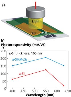
Sayeef Salahuddin and Mohammad Esmaeili-Rad solved this problem by pairing a thin film of MoS2 with a sheet of a-Si. By forming a diode with the a-Si, the MoS2 allows the photogenerated electrons it collects to travel ten times faster through the a-Si. The detector has a photoresponsivity of 210 mA/W for green light—two to four times higher than usual for a-Si devices.
The researchers say that because these materials are easy and inexpensive to handle, the cost of speeding up photodetectors would be minimal. Unlike conventional semiconductors like Si, MoS2 consists of individual nanosheets that can be torn off like pages in a book. These sheets can be used to make thin, novel electronic devices or to improve existing ones.
Mechanically peeled flake
The structure consists of a 60-nm-thick mechanically exfoliated (peeled) MoS2 flake on a silicon dioxide (SiO2) substrate, with the flake covered by a 100-nm-thick a-Si film using plasma-enhanced chemical vapor deposition (see figure). Gold (Au) and titanium contacts were also added via electron-beam evaporation. A control device without the MoS2 flake was also fabricated.
The photoresponse of the devices was measured using standard blue, green, and red LEDs as light sources at an incident power of about 0.4 mW/cm2. The photoresponse to light from the three LEDs was much higher for the MoS2-containing device. The response of the detectors to transients was also measured, showing a 3 to 5 ms residual conductivity for the a-Si devices but a lack of this residual response in the MoS2-containing detector. As a result, say the researchers, the imaging speed of the new detector is increased by a factor of ten over the conventional a-Si detector.
This new photodetector structure could be used in large-area biomedical imaging, the researchers note. In one example, the fast response of the a-Si/MoS2 photodetector could allow flat-panel x-ray imagers to reach frame rates of up to several kilohertz—much faster than the 10 to 1000 Hz frame rates of conventional a-Si-based x-ray imagers. But for practical use, large-area fabrication approaches such as chemical vapor deposition should be developed, replacing mechanical exfoliation. Ultimately, integration with MoS2 transistors could be achieved, leading to large monolithic optoelectronic imaging devices.
REFERENCE
1. M. R. Esmaeili-Rad and S. Salahuddin, Sci. Rep., 3, 2345 (Aug. 2, 2013); doi:10.1038/srep02345.

John Wallace | Senior Technical Editor (1998-2022)
John Wallace was with Laser Focus World for nearly 25 years, retiring in late June 2022. He obtained a bachelor's degree in mechanical engineering and physics at Rutgers University and a master's in optical engineering at the University of Rochester. Before becoming an editor, John worked as an engineer at RCA, Exxon, Eastman Kodak, and GCA Corporation.
