CMOS SENSORS: CMOS-based specialty imagers reach new performance levels

ELS PARTON, JEROME BARON, and PIET DE MOOR
Complementary metal-oxide semiconductor (CMOS) imagers have largely replaced charge-coupled device (CCD) imagers in smartphones and digital cameras due to lower costs and higher integration capability. But for medical applications, microscopy, space applications, and machine vision, CCD imagers are still dominating the market; that is, the market share of CMOS in these fields is estimated at only 10–15% due to performance issues.
In response, imec researchers are developing CMOS imagers that are as good as and even better than CCD imagers for high-end applications. More specifically, up to 1000X increases in speed and sensitivity to wavelengths beyond the visible region exemplify the accomplishments to date.
Optical layer innovations
In a specialty imager, optical layer optimization is paramount to performance. Antireflective coatings maximize the penetration of light into the sensitive silicon by minimizing the reflectance at the imager surface. When detecting nonvisible ultraviolet (UV) light, the designer needs to consider the absorption of light in the dielectric materials in the layers above the silicon, as well as the very shallow penetration of UV light into silicon.
For the detection of extreme ultraviolet (EUV) light, we use a very thin boron (B) passivation coating that has minimal absorption and also provides stable operation of the imager under high radiation doses. This technology enables, for example, dose monitoring in advanced lithography equipment.
Hyperspectral filters offer added dimensions to CMOS imagers for applications in industrial inspection, anticounterfeiting, food quality control, and medical applications such as skin-cancer screening. Imec researchers have developed a hyperspectral imager by integrating a group of 100 spectral filters, arranged in the shape of a wedge, on top of a commercial CMOS imager. The result is a compact and fast hyperspectral camera made with mass-producible and fully CMOS-compatible process technology.
The integrated spectral filters are narrowband Fabry-Pérot interference filters. The Fabry-Pérot filter is typically made of a transparent layer (cavity) with a mirror at each side. The length of the cavity defines the central wavelength of the optical filter, and the reflectivity of the mirrors defines the full-width half-maximum (FWHM) of the filter.
Using these filters, different hyperspectral imager designs can be realized. As an example, a line scan hyperspectral imager can record a full three-dimensional (3D) data cube for a linear moving object. The hyperspectral filters can be processed in principle on any image sensor to match the specifications required for different applications. Similarly, the spectral range can be tuned, and currently an extended spectral range of 400-1000 nm is under development.
A better read-out circuit
Using our expertise in analog-to-digital converters (ADCs), we have developed new imager designs that enable fast readout of large imagers with low power consumption. Next-generation high-resolution televisions will feature eight times more pixels and will be read out at a speed of up to 120 frames/s.
In traditional imagers, the pixels are read out per column and then the data is multiplexed to one ADC. If instead one ADC per imager column is used, the digitalization is parallelized, resulting in a higher frame rate with lower power consumption. We recently demonstrated a column-based, 12-bit ADC using a sigma-delta architecture. This design allowed read out of an 8 Mpixel imager at a speed of 60 frames/s.
In terms of circuitry integration, our embedded CCD (eCCD) technology combines the best of both worlds: the electro-optical performance of CCDs in combination with the complexity and the speed of CMOS readout electronics. By adding a CCD module to our 0.13 μm CMOS process flow, we have both CCD-like pixels and CMOS readout electronics in one device. One of the critical parameters for proper operation of the CCD pixels is the submicron spacing (approximately 150 nm) between the electrodes-a parameter achieved through advanced lithography. The eCCD module enables custom design depending on application needs and is compatible with backside illumination (BSI).
One eCCD application example is time delay integration (TDI) imagers. The charge transfer in the CCD pixels results in a noiseless transfer and integration synchronized with the moving scene-something that is very difficult to achieve using CMOS imagers. eCCD technology also enables imaging at extremely high speeds (up to 1 billion frames/s); in this case, a large number of images (around 100) are stored inside the pixels using CCD elements as analog memories. After acquiring 100 images at very high speed, the pixels can be read out in a similar way as in a traditional imager. This burst-mode imaging is used in scientific applications such as fluid dynamics.
Building the best pixel
In a typical front-side-illuminated imager, the light enters the optical layers and passes through the so-called 'back-end-of-line' consisting of metal and dielectric layers, before reaching the light-sensitive silicon. Since the back-end-of-line materials reflect and even absorb part of the light, a good way to reach high quantum efficiency (QE) is to enable BSI.
In BSI imagers, the silicon substrate is removed, and the light directly enters the imager from the backside. These BSI CMOS imagers require advanced wafer bonding, grinding, chemical-mechanical polishing, selective wet etching, and laser annealing. In a BSI imager, there is a direct transition from air to silicon (without the back-end-of-line layers in between) and, therefore, the fill factor is 100% and the QE enhanced. Also, contrary to frontside illuminated imagers, BSI imagers are sensitive to UV light.
Another method we are exploring is the use of dedicated substrates for fabricating improved CMOS specialty imagers. For example, by using a thick layer of sensitive silicon, near-infrared (NIR) response can be increased since for NIR wavelengths the penetration depth of photons is rapidly increased. However, this typically leads to worsening pixel crosstalk; that is, a degradation in the effective imager resolution. To counteract this crosstalk effect, one solution is our use of special substrates with a graded dopant concentration that guides the charges created by the absorbed photon towards the nearest pixel. Another solution is to isolate pixels using a trench, which prevents the charges from moving to a neighboring pixel.
In order to manufacture large-area imagers, two different technologies can be used.
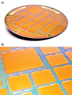
As the mask area typically allows maximum chip sizes of about 2 × 2 cm2, a special technique called stitching is required for the realization of larger imager devices (see Fig. 1). In this case, sub-blocks (different components of the imager) are repeatedly printed on the wafer to develop small and large imager devices.
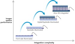
Another technology is butting: individual imager chips are mounted closely together to form one big imager device. However, since the imagers cannot be mounted without leaving a gap between, a non-sensitive area is created. This so-called dead area can be minimized using 3D stacking technology in which wire bonds are replaced with through-silicon vias (TSVs) that allow a vertical input/output connection structure that largely minimizes the dead area. Large-area imaging is useful for such applications as X-ray medical imaging.Finally, 3D integration also enables complete new imager architectures; for example, having backside-illuminated pixels on the first wafer and readout circuitry on the second. This hybrid backside illuminated imager architecture enables more flexible integration by dissociating the processing of both layers to enable smart and/or high-speed imagers (see Fig. 2).
Els Parton is scientific editor; Jerome Baron is product marketing manager, imaging; and Piet De Moor is program manager, optical sensors at imec, Kapeldreef 75, B-3001 Leuven, Belgium; email: [email protected]; http://www.imec.be
