LASER-DRIVEN PARTICLE ACCELERATORS: On-chip DLA is precursor to tabletop particle accelerator

Stanford University (Stanford, CA), SLAC National Accelerator Laboratory (Menlo Park, CA), University of California, Los Angeles (UCLA; Los Angeles, CA), and Tech-X Corporation (Boulder, CO) researchers have demonstrated high-gradient (beyond 250 MeV/m) acceleration of electrons in a 550-μm-long microfabricated dielectric laser accelerator (DLA).1 In contrast, conventional linear accelerators operate at gradients from 10 to 30 MeV/m, and the very first linear radiofrequency design achieved 1.6 MeV/m in a 1-m-long cavity.
The researchers say that laser-driven, multistaged integration of on-chip DLA devices could enable tabletop accelerators on the megaelectron- to gigaelectron-volt scale for security scanners and medical therapy devices, as well as compact x-ray light sources for biophotonics research, and could reduce the size and cost of multiteraelectron-volt (1012 eV), laser-driven particle accelerators.
DLA structures
For successful laser-driven particle acceleration, the electric field of the laser must have a component parallel to the electron-beam trajectory and a phase velocity matching the relativistic particle-beam velocity. The researchers accomplished this through a lithographically fabricated, fused-silica grating accelerator structure operating in the commercially available Ti:sapphire (800 nm) laser window.
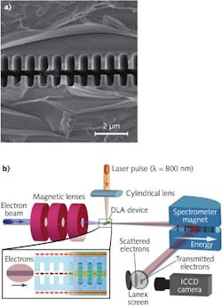
The DLA structure is essentially two 550-μm-long opposing binary gratings with an 800 nm period and separated by a gap through which the electrons travel (see figure). The electron beam travels perpendicular to the grating rulings, while the linearly polarized laser pulse is incident perpendicular to the electron-beam direction and perpendicular to the plane of the gratings. Essentially, the DLA structure acts like a longitudinally periodic phase mask, with phase synchronicity achieved by matching the grating period to the laser wavelength. Electrons injected into the laser field experience both acceleration and deceleration since the duration of the electron beam (429 ± 31 fs) is much longer than the laser optical cycle (2.6 fs).
In experiments at SLAC, a 60 MeV electron beam is magnetically focused to a 24 × 8 μm spot size and partially transmitted through DLA structures with gap widths of both 400 nm and 800 nm. The 400 nm gap-width structure offers higher acceleration gradients, but places a tighter tolerance on the electron beam. The electron beam interacts with the 30 × 300 μm root-mean-squared (RMS) spot size of the Ti:sapphire laser with a pulse length of 1.24 ± 0.12 ps. For this configuration, with only 2.2% of the 60 MeV beam transmitted through the 400 nm gap-width DLA gratings, measured acceleration gradients reached up to 310 MeV/m at the maximum available laser power. This is 6–10 times higher than typical operating gradients in conventional radio-frequency (RF) structures.
“For a proof-of-principle experiment, our results are very promising, and if we optimize the structure geometry and the drive laser pulse we should be able to reach GeV/m gradients,” says Edgar Peralta, a graduate student at Stanford University. “However, this is only the first step towards building a fully functional DLA-based accelerator or x-ray source. There are other required components we still need to demonstrate, such as focusing and deflecting structures, but we are hopeful that their development and integration can take place over the next decade.”
REFERENCE
1. E. A. Peralta et al., Nature, doi:10.1038/nature12664, or see http://www.nature.com/nature/journal/vnfv/ncurrent/full/nature12664.html (2013).

Gail Overton | Senior Editor (2004-2020)
Gail has more than 30 years of engineering, marketing, product management, and editorial experience in the photonics and optical communications industry. Before joining the staff at Laser Focus World in 2004, she held many product management and product marketing roles in the fiber-optics industry, most notably at Hughes (El Segundo, CA), GTE Labs (Waltham, MA), Corning (Corning, NY), Photon Kinetics (Beaverton, OR), and Newport Corporation (Irvine, CA). During her marketing career, Gail published articles in WDM Solutions and Sensors magazine and traveled internationally to conduct product and sales training. Gail received her BS degree in physics, with an emphasis in optics, from San Diego State University in San Diego, CA in May 1986.