SEMICONDUCTING POLYMERS: Polymer retinal implant is totally self-contained
A group of researchers from the Jawaharlal Nehru Center for Advanced Scientific Research (Bangalore, India) and Tel Aviv University (Tel Aviv, Israel) has created a polymer-based active photosensitive platform intended as a simple, wiring-free “epiretinal” implant to restore a measure of vision to blind people.1 Tested on an embryonic-stage blind chick retina, the approach is simpler than conventional approaches using inorganic photodiode arrays and electrodes.
The implant is based on semiconducting conjugated-polymer-based bulk heterojunctions (BHJs), which are thin, flexible, and highly light-absorbent. In addition, these devices are biocompatible and can be made using solution-processing techniques. Setting out to develop implants that can bring sight with endogenous blind retinas, the researchers developed a photoactive BHJ layer with high quantum efficiency that could be coated on a commercial multielectrode array (MEA). The entire device operates without any external power and, thus, without the need for wires. Endogenous blindness involves “degeneration of the light-sensitive photoreceptor layer of the retina, while the other retinal circuitry is preserved,” says K. S. Narayan, the lead researcher. “The present efforts are directed towards eliciting visual perception in such specific cases.”
Control and background experiments consisted of photoexciting 1) a blind chick retina placed against an MEA that has no BHJ film; 2) a BHJ-coated MEA in a buffer medium with no chick retina; and 3) an MEA with no BHJ coating and no chick retina in a buffer solution. The researchers confirmed that without a BHJ film, the MEA produced no neuronal response in the blind chick retina. For the BHJ-coated MEA with no retina, photoexcitation produced a rising voltage (measured via the MEA) with light and a voltage decay with the removal of light. This action occurred for monochromatic light at 533 nm (55 μW/cm2) and 575 nm (97 μW/cm2), and for white light (200 μW/cm2).
Similar to natural eye response
With a retina in place, the BHJ-coated MEA produced neuronal retinal responses measured on about 10% of the electrodes. The researchers believe this percentage can be raised with better fabrication to ensure good contact between the BHJ and MEA across the device. Retinal responses were similar to the natural response of a retina to photostimulation. Varying wavelengths, light intensities, and pulse durations were tested.
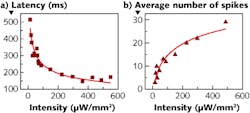
The induced neuronal response shows itself as spikes that increase in rate with increasing light intensity, and whose latency decreases with increasing intensity (see figure). The BHJ implant material absorbs light from about 400 to 600 nm; the retina responded over this same range. The researchers also tested the spatial resolution using a 200-μm-diameter light spot; some localized response could be seen, even when the spot was 500 μm away. The researchers attribute this to scattering within the structure supporting the retina.
Voltage response of the device can be tuned by varying the thickness and makeup of the BHJ layer, say the researchers. With the addition of transparent electrodes and a conformable substrate, this sort of device could become a totally self-contained retinal prosthesis that would alleviate common retinal diseases such as age-related macular degeneration and retinitis pigmentosa.
“The advent of semiconducting plastic technology should be promising for advanced bioelectronic and neuroprosthetic interfaces,” says Narayan. “The possibility of seamlessly integrating the sensory world with the environment is an exciting possibility. It is a long road ahead to realize the possible utility of biocompatible organic optobioelectronics.”
REFERENCE
1. V. Gautam et al., Adv. Mater., doi:10.1002/adma.201304368 (2013).

John Wallace | Senior Technical Editor (1998-2022)
John Wallace was with Laser Focus World for nearly 25 years, retiring in late June 2022. He obtained a bachelor's degree in mechanical engineering and physics at Rutgers University and a master's in optical engineering at the University of Rochester. Before becoming an editor, John worked as an engineer at RCA, Exxon, Eastman Kodak, and GCA Corporation.
