Photonics Applied: Laser Additive Manufacturing: How does additive manufacturing 'stack up' against subtractive methods?
When Laser Focus World wrote about laser additive manufacturing in its Photonics Applied series back in 2009, the phrase "3D printing" was not even mentioned. Fast-forward to 2014, and 3D printing is one of the hottest manufacturing trends, with a market size forecast to reach $4.5 billion by 2018, according to Global Industry Analysts (GIA; San Jose, CA).1 Similarly, Wohlers Associates (Fort Collins, CO) says sales of additive manufacturing equipment and related services reached $2.2 billion in 2012 and should rise to $6 billion by 2017.2
In May 2013, a .38 caliber bullet was fired from the first fully 3D printed gun dubbed "the Liberator" by its creator Cody Wilson, founder and director of Defense Distributed (http://defdist.org), a non-profit organization 'empowering' the public through 3D-printed firearms. Concerning the method of manufacture, Andy Greenberg of Forbes online revealed, "Unlike the original, steel Liberator, though, Wilson's weapon is almost entirely plastic: Fifteen of its 16 pieces have been created inside an $8,000 second-hand Stratasys Dimension SST 3D printer … The only non-printed piece is a common hardware store nail used as its firing pin."3
The problem for the photonics industry, however, is that Stratasys (Eden Prairie, MN, and Rehovot, Israel) 3D printers don't use lasers—they use heat to cure thermoplastics. It is therefore extremely important to recognize that not all 3D printing systems are laser-based. The hype surrounding 3D printing has more to do with low-cost, heat-based, nozzle-extruded-polymer systems for in-home and small-shop use than it does with the more-expensive, higher-resolution, and higher-component-quality laser additive manufacturing (LAM) systems that this feature article addresses.
With many names and technology variations such as laser AM, laser melt deposition, selective laser melting (SLM), vat photopolymerization, laser sintering or cusing, direct metal laser sintering (DMLS), or laser 3D printing, LAM industry success is contingent upon the fabrication of physical component parts that can meet or exceed the strength, durability, manufacturing ease, and cost/volume targets of components fabricated using traditional subtractive manufacturing methods such as machining and molding, or even competing electron beam melting (EBM) technology. So just how do LAM components compare to conventional fabricated parts?
Metal components
The trademarked LaserCUSING process from Concept Laser (Lichtenfels, Germany) can be used with stainless and tool steels, aluminum and titanium alloys, nickel-based superalloys, cobalt-chromium alloys, or precious metals such as gold or silver alloys. The company opened a 600 m2R&D facility in late 2013 in response to growing demand for laser additively manufactured components for jewelry, dental implants, and even automotive and aerospace components.
With fiber laser power levels up to 1 kW (and multi-laser systems on the way), Concept Laser's powder-bed-based components (see http://bit.ly/1gxjF18) are built up in layers with thicknesses from 15 to 200 μm and powder-bed dimensions ranging from 5 cm wide and deep and 8 cm tall to a current maximum of 63 cm wide, 40 cm deep, and 50 cm tall, with a build rate that varies from 1 to 100 cm3/hr. Dental restoration manufacturer Unicim (Berschis, Switzerland) uses a Concept Laser Mlab Cusing R system with a 100 W continuous-wave (CW) fiber laser to create metal (such as titanium) dental implants that the company says are superior—qualitatively—to milled components in terms of density and lack of distortion.
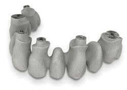
Renishaw (Wotton-under-Edge, England) says its LAM-built cobalt chrome LaserBridges have high precision and super occlusal detail, are stress-relieved for accuracy, and offer excellent porcelain retention (see Fig. 1). The AM250 laser melting machine from Renishaw uses a 200 or 400 W ytterbium fiber laser with a 70 μm beam diameter at the surface of a 25 × 25 × 30 cm powder bed to deposit 20- to 100-μm-thick layers that can build a 5 to 20 cm3 component in one hour.
In short, many dental implant companies are anticipating the demise of casting and milling/machining in favor of more cost-effective LAM-built implants, and for good reason: A May 2013 research study in Lasers in Medical Science evaluated the reliability and failure modes of dental implants fabricated via machining (surface treated with alumina blasting/acid etching) and laser sintering for anterior single-unit replacements.4 After subjecting a total of 42 implants (21 in each group) to step-stress accelerated life testing and performing polarized-light and SEM fractographic analysis, no differences in reliability and fracture mode were observed between machined and laser-sintered implants.
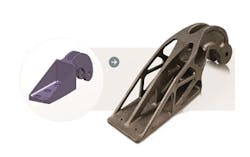
SmarTech (Charlottesville, VA) estimates that the market for 3D printed medical and dental products alone will reach $2.8 billion by 2019.5 But what about more sophisticated metal components that are subjected to much harsher environments than the human mouth? In July 2013, NASA finished testing a rocket engine injector made through selective laser melting by Aerojet Rocketdyne (West Palm Beach, FL). Firings of a liquid oxygen and gaseous hydrogen rocket injector assembly demonstrated the integrity of this highly critical rocket engine component, and perhaps more importantly, NASA said that injectors fabricated using traditional processes would take more than a year vs. only four months—at a 70% cost reduction-for 3D-printed components.In addition to cost reduction, LAM components for aerospace applications (see http://bit.ly/1dHV7PP) may have another significant benefit: weight reduction. In a case study reported by additive systems manufacturer EOS (Novi, MI) and conducted by EADS Innovation Works (EADS IW; Bristol, England), traditional Airbus A320 steel-cast nacelle hinge brackets were compared to titanium brackets with optimized topology using EOS DMLS technology (see Fig. 2).6 The EADS IW energy consumption analysis included not only the production steps, but also the sourcing and transport of raw materials, and argon consumption and waste produced for the atomization process of the metal powder material. For the whole lifecycle of the components, including static manufacturing and operational phases of the brackets, the study revealed a 40% reduction in energy consumption, a 25% reduction in raw material consumption, and a potential weight savings per plane of around 10 kg.
Polymer and ceramic components
In February 2013, Oxford Performance Materials (OPM; South Windsor, CT) received the first FDA 510(k) clearance for polymer laser-sintered OsteoFab Patient-Specific Cranial Device (OPSCD) implants-custom devices fabricated from biocompatible, chemically inert, and radiolucent poly-ether-ketone-ketone (PEKK) thermoplastic that restore voids in the skull caused by trauma or disease.Low tooling costs, reduced waste, and customization capability made additive manufacturing a logical choice for cranial implant fabrication. However, the high melting point of PEKK (360°C) precluded the use of thermal 3D printers and instead required the higher-energy laser sintering capabilities of a system like the high-temperature EOSINT P 800 laser-sintering system from EOS.
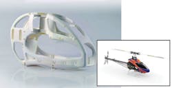
Although the EOSINT P 800 combines two 50 W CO2 lasers to build 120-μm-thick layers, the EOS P 396 for medium-build-volume jobs creates layers from 60 to 180 μm thick (depending on the application and powder material used), and was the choice for Mikado Model Helicopters (Potsdam, Germany) to fabricate housings for its model helicopters using polyamide PA 2200 material with 60 μm average particle size (see Fig. 3).To address the finer details needed for many components in the micromachining category, EOS and 3D-Micromac (Chemnitz, Germany) recently formed a new company called 3D MicroPrint that will manufacture LAM systems using lasers with ≤ 30 μm focus diameters to build layer thicknesses of ≤ 5 μm from powders with particle size ≤ 5 μm.
To obtain a more compact powder bed for selective laser sintering of ceramics, the BAM Federal Institute for Materials Research and Testing (Berlin, Germany) does not deposit a dry powder, but instead uses a powder suspension (known as a 'slip' or 'slurry' in the ceramics industry) that incorporates sub-micrometer-sized particles to achieve a 65%-of-theoretical packing density. The proprietary process (Patent US 6,827,988 B2) called Layerwise Slurry Deposition (LSD) has been implemented in BAM's own LSD 100 system that deposits slurry layers, dries them, and applies fiber laser energy at 1034 nm (100 W CW) and 1940 nm (50 W CW) to create laser-sintered ceramic components.
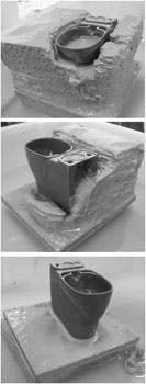
"The fine ceramic slurry allows us to tune the interaction of the laser light with the powder's particle size so that the penetration depth of the laser light into the material bed can be adjusted," says Jens Günster, head of BAM's Ceramic Processing and Biomaterials division.7 "Furthermore, due to the high density of the slurry bed, we don't need to build up support structures as the bed itself provides sufficient support." With process time comparable to subtractive technologies even including the somewhat time-intensive slurry washing process, BAM can create objects such as sanitary silicate ceramic toilets with a microstructure comparable to bisque-fired objects (see Fig. 4).
Component integrity
Powder particle sizes are largely responsible for the finished surface quality and density of LAM-fabricated components, and are even the subject of an ASTM Standard Guide in development on particle characterization being supported by the National Institute of Standards and Technology (NIST) for the benefit of LAM system users and manufacturers.
"Many laser-based, powder bed fusion systems typically have mean metal particle sizes between 20 and 40 μm, but the powder also contains bigger and smaller particles," says John Slotwinski, physicist at NIST's Production Systems Group in Gaithersburg, MD. "Having a distribution of sizes is important because it allows the particles to pack better on the build plate; the gaps become filled with the smaller particles, reducing porosity."
Numerous industrial, corporate, and university research groups such as The Welding Institute (TWI; Cambridge, England), the Additive Manufacturing Consortium (Columbus, OH), Joining Technologies (East Granby, CT) in partnership with Fraunhofer ILT (Aachen, Germany), the Beijing University of Aeronautics and Astronautics (Beijing, China), and Pennsylvania State University (Penn State or PSU; University Park, PA) are actively engaged in understanding LAM methods and how particle sizes, laser energy, and other manufacturing parameters affect the end component.
"Our current research is primarily directed at understanding and developing improved processes that reduce distortion and residual stress, for example, in metallic—especially titanium and nickel-based alloy—components fabricated using laser and electron beam deposition techniques," says Todd A. Palmer, senior research associate and associate professor of Materials Science and Engineering in Penn State's Applied Research Laboratory. Palmer says that while LAM is compelling for producing components with unique geometries that don't lend themselves to traditional machining or molding, the LAM process still cannot produce parts with forged properties. "Follow-on processes, such as heat treatment or hot isostatic processing are necessary to bring these components closer to the properties seen in traditional cast-forge processing routes."
Palmer cautions that LAM components also display significant anisotropy in the material properties and often, defects such as a lack of fusion porosity that negatively impact fatigue properties of the finished component. "There are a lot of mechanical properties reported in the literature, but in most cases, the processing parameters used to produce the components are not well established or referenced," adds Palmer. "We have current efforts underway to identify the essential variables for the different AM processes that will allow this necessary process pedigree to be obtained."
REFERENCES
1. See http://bit.ly/1iChIC8.
2. See http://bit.ly/1j1qDzL.
3. See http://onforb.es/1aueWwN.
4. E. O. Almeida et al., Lasers Med. Sci., 28, 3, 851–858 (May 2013).
5. See http://bit.ly/1adR0gF.
6. See http://bit.ly/19mKplW.
7. T. Mühler et al., Int. J. Appl. Ceramic Technol., doi:10.1111/ijac.12113 (May 13, 2013).

Gail Overton | Senior Editor (2004-2020)
Gail has more than 30 years of engineering, marketing, product management, and editorial experience in the photonics and optical communications industry. Before joining the staff at Laser Focus World in 2004, she held many product management and product marketing roles in the fiber-optics industry, most notably at Hughes (El Segundo, CA), GTE Labs (Waltham, MA), Corning (Corning, NY), Photon Kinetics (Beaverton, OR), and Newport Corporation (Irvine, CA). During her marketing career, Gail published articles in WDM Solutions and Sensors magazine and traveled internationally to conduct product and sales training. Gail received her BS degree in physics, with an emphasis in optics, from San Diego State University in San Diego, CA in May 1986.


