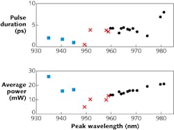
Near-infrared vertical external-cavity surface-emitting lasers (VECSELs) are typically modelocked with semiconductor saturable absorber mirrors (SESAMs). An alternative method for modelocking, however, uses a graphene saturable absorber mirror (GSAM). Researchers from ETH Zurich (Zurich, Switzerland), the University of Cambridge (Cambridge, England), and Sungkyunkwan University (Suwon, South Korea) report a 21 nm tuning range from a GSAM-modelocked VECSEL—a value that exceeds the capabilities of recently reported SESAM-modelocked VECSELs.
The GSAM is prepared by CVD growth of a single-layer graphene sheet. The 100 mm2 sheet is then transferred to a distributed Bragg reflector (DBR) with high reflectivity from 930 to 1010 nm. VECSEL gain chips with center wavelengths at 940 nm (blue squares), 950 nm (red x symbols), and 970 nm (black circles) were then arranged in a folded-mirror cavity with a high-reflectivity mirror, output coupler mirror, GSAM as end mirror, and an intracavity etalon used as the tuning mechanism. The 970 nm gain structure exhibits the broadest tuning range of 21 nm, with 13–21 mW average output power. Stable modelocking is observed for all the structures at a 1.5 GHz repetition rate, with pulses as short as 473 fs (without the etalon). Using the three different VECSEL chips, the tuning range can be extended to 46 nm. Contact Christian A. Zaugg at [email protected].

Gail Overton | Senior Editor (2004-2020)
Gail has more than 30 years of engineering, marketing, product management, and editorial experience in the photonics and optical communications industry. Before joining the staff at Laser Focus World in 2004, she held many product management and product marketing roles in the fiber-optics industry, most notably at Hughes (El Segundo, CA), GTE Labs (Waltham, MA), Corning (Corning, NY), Photon Kinetics (Beaverton, OR), and Newport Corporation (Irvine, CA). During her marketing career, Gail published articles in WDM Solutions and Sensors magazine and traveled internationally to conduct product and sales training. Gail received her BS degree in physics, with an emphasis in optics, from San Diego State University in San Diego, CA in May 1986.
