Laser-induced dumbbell air voids increase LED output
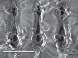
Using an ultrafast picosecond pulsed laser, researchers at the Institute of Semiconductors at the Chinese Academy of Sciences (Beijing, China) have successfully formed laser-microstructured, dumbbell-shaped air voids inside the sapphire substrates of indium gallium nitride (InGaN) light-emitting diodes (LEDs) that improve the light output power of packaged devices by 24.7%. The noncontact technique, which increases light scattering at the sapphire/void interface, borrows from other light-enhancing methods that up to now have been achieved using more-complicated laser micromachining or nanostructuring techniques.
The voids are fabricated using a 1 W, 1064 nm laser with 15 kHz repetition rate and 50 ps pulse duration focused at a depth of 100 μm in roughly the center of the sapphire substrate. Analysis of the sapphire structure using microscopy and far-field radiation patterns showed vertically stacked air voids with upper and lower diameters of 1.2 and 0.5 μm, respectively. A ray-transfer matrix analysis reveals that the dumbbell shape is the result of a local change in refractive index at the first void location that creates a secondary focus effect of the laser beam that in turn creates the second void. In addition to increased light output from the rapid and inexpensive process, leakage currents were slightly lower for the air-void devices compared to conventional devices, meaning that the process does not degrade the electrical performance of the LEDs. Contact Xiaoyan Yi at [email protected].
About the Author

Gail Overton
Senior Editor (2004-2020)
Gail has more than 30 years of engineering, marketing, product management, and editorial experience in the photonics and optical communications industry. Before joining the staff at Laser Focus World in 2004, she held many product management and product marketing roles in the fiber-optics industry, most notably at Hughes (El Segundo, CA), GTE Labs (Waltham, MA), Corning (Corning, NY), Photon Kinetics (Beaverton, OR), and Newport Corporation (Irvine, CA). During her marketing career, Gail published articles in WDM Solutions and Sensors magazine and traveled internationally to conduct product and sales training. Gail received her BS degree in physics, with an emphasis in optics, from San Diego State University in San Diego, CA in May 1986.
