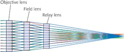
A compound lens consists of an array of lenslets, similar to the type of eye optics that insects have; a Gabor superlens (GSL) is a type of compound lens in which all the images created by the lenslets in an array coincide to create a single large image. A GSL consists of two or more individual lenslet arrays spaced an axial distance from each other to form a lightweight array of multielement lenslets; the array periods are slightly different so that all the multielement lenslets share the required common focal point. As might be expected, the lenslets toward the edge of the array show greater aberrations then those near the center.
R. Hamilton Shepard of Massachusetts Institute of Technology’s Lincoln Laboratory (Lexington, MA) has characterized the third-order (Seidel) aberrations of example two- and three-element Gabor superlenses; the results, although they neglect higher-order aberrations, should offer lens designers an intuitive look into the design and performance of GSLs. Results were confirmed by comparing theory to ray traces, and show that the third-order lenslet-array-position-dependent aberrations are scaled versions of the aberrations shown by the center multielement lenslet. Shepard notes that these aberrations could be improved by minimizing aberrations in the relay lenslets (for the two-array GSL) and the field and relay lenslets (for the three-array GSL), as opposed to trying to balance their aberrations with the first (objective lens) array, as designers might conventionally try to do. Contact R. Hamilton Shepard at [email protected].

John Wallace | Senior Technical Editor (1998-2022)
John Wallace was with Laser Focus World for nearly 25 years, retiring in late June 2022. He obtained a bachelor's degree in mechanical engineering and physics at Rutgers University and a master's in optical engineering at the University of Rochester. Before becoming an editor, John worked as an engineer at RCA, Exxon, Eastman Kodak, and GCA Corporation.
