Terahertz Imaging: Terahertz microscope images chemical reactions
Using an imaging process they call laser-terahertz emission microscopy (LTEM), researchers at Okayama University (Okayama, Japan) have developed a terahertz chemical microscope (TCM) that images chemical reactions with higher spatial resolution than conventional terahertz imaging methods.1 That is, the TCM spatial resolution is not limited by the wavelength of the terahertz radiation generated, but instead is limited by the much shorter wavelength of the femtosecond laser used to generate the terahertz radiation.
Terahertz sensing
The reactive portion of the TCM consists of thin silicon dioxide (SiO2) and silicon (Si) layers (275 and 170 nm thick, respectively) on a sapphire substrate. When light from a 790-nm-emitting femtosecond laser operated with a 100 fs pulse width and an 82 MHz pulse repetition rate travels through the sapphire substrate and strikes the Si-based films, terahertz radiation with a peak wavelength of approximately 0.3 THz is generated and radiated to a low-temperature-grown gallium arsenide (GaAs) photoconductive antenna sensor that works as the terahertz detector.
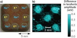
If a chemical reaction progresses on the 10 mm2 sensing plate above the film, chemical and/or electrical potential shifts at the surface of the plate cause a change in the local field magnitude and a corresponding variation in the amplitude of the generated terahertz pulse. And because the terahertz pulse contains information about the reaction at the precise location of the laser that created the pulse, scanning the laser across the sensing plate produces a map or image of the spatial details of the chemical reaction (see figure).
Although the spatial resolution of the TCM is currently about 50 μm, this can be improved by optimizing the aperture of the objective lens that is used to focus the laser onto the sapphire substrate. Currently, a plano-convex lens with a diameter of 25.4 mm and focal length of 60 mm is used, where the spot size of the laser was approximately 3 mm.
Possible reactions
Currently, the TCM system can be used to detect changing concentration levels of ions in solution, or changes in immunoglobulin reactions. The researchers say that the label-free technique is even more sensitive than standard immunoassays because the TCM process is not dependent on the molecular weight of the sample; for example, they have been able to detect molecules as small as biotin that are difficult to measure using conventional methods.
“Now, we are working toward realizing a ‘multi-omics’ platform using TCM for a next-generation medical diagnostic system,” says Toshihiko Kiwa, associate professor at Okayama University. Multi-omics (or multiomics) is defined as being applicable to multiple fields of study ending in the phrase ‘omics,’ such as genomics and proteomics. “We already developed the prototype TCM and sensing plates are ready to deliver to researchers in diverse research fields who are interested in screening and/or visualization of chemical or bioreactions,” Kiwa adds.
In addition to exploring TCM applications in medical diagnosis and materials research, the researchers are also developing fuel cells that will be mounted on the sensing chip so that catalytic reactions of their electrodes can be measured.
REFERENCE
1. T. Kiwa et al., “Imaging chemical reactions,” SPIE Biomedical Optics & Medical Imaging online (December 31, 2013).

Gail Overton | Senior Editor (2004-2020)
Gail has more than 30 years of engineering, marketing, product management, and editorial experience in the photonics and optical communications industry. Before joining the staff at Laser Focus World in 2004, she held many product management and product marketing roles in the fiber-optics industry, most notably at Hughes (El Segundo, CA), GTE Labs (Waltham, MA), Corning (Corning, NY), Photon Kinetics (Beaverton, OR), and Newport Corporation (Irvine, CA). During her marketing career, Gail published articles in WDM Solutions and Sensors magazine and traveled internationally to conduct product and sales training. Gail received her BS degree in physics, with an emphasis in optics, from San Diego State University in San Diego, CA in May 1986.
