Chirped Pulse Amplification: Three-level mask repeatably creates pulse-compression gratings
Chirped pulse amplification (CPA) has enabled the creation of ultrafast lasers with high pulse energies and very short pulse lengths. In CPA, a short seed pulse (which, as a result of the pulse’s brevity, has a wide wavelength band) is dispersed by diffraction gratings, greatly stretching the pulse so that it can be amplified without harming the gain medium. After amplification, a second set of gratings recompresses the pulse.
Fabricating the pulse-compression gratings for CPA can be done using electron-beam lithography (EBL) and reactive ion etching, but this process is both slow (on the scale of hours for a single wafer) and expensive. Interference lithography, which relies on two interfering laser beams to expose a grating in resist, is not stable enough to create a number of identical pieces in series.
Aiming to create a robust, repeatable, inexpensive process for fabricating CPA gratings, researchers at Friedrich Schiller University and the Fraunhofer Institute for Applied Optics and Precision Engineering (both in Jena, Germany) have developed a technique based on i-line (365 nm) proximity photolithography, performed in a simple mask aligner.1 The computer-optimized, three-level phase mask used to create the aerial images ensure high resolution and a large depth of focus (the mask itself is fabricated using EBL).
The three-level phase-mask profile results from an optimization that uses rigorous coupled-wave analysis to calculate the physical mask transmission, says Lorenz Stuerzebecher, one of the researchers. “The merit for the optimization is defined by both the similarity of the realized transmission to the ideal complex field to be synthesized and fabrication constrains,” he notes. “No empirical refinement is necessary.”
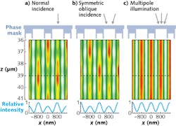
If illuminated only at normal incidence, the resulting phase mask produces an aerial image that creates an undesirable “beating” effect (see figure). However, if illuminated at symmetric oblique incidence, a beating effect occurs that alternates in the opposite way. Combining the two by using multipole illumination creates a consistent aerial image.
Black-chrome substrate
Aiming to make CPA gratings with an 800 nm period, the researchers first had a 6 in. phase mask fabricated; the mask actually had a 1600 nm period with some sub-period structure. Fused-silica wafers 1 mm thick with a low-reflective chromium (LR-Cr, or “black chrome”) coating were used as the pulse-compression-grating substrate, coated with a 370-nm-thick layer of photoresist and placed 38.5 μm away from the phase mask.
After exposure, inductively coupled plasma (ICP) etching created the gratings; the large difference in etching speed between the silica and the black chrome enabled the creation of high-aspect-ratio ridges in the silica. In the last step, the remaining LR-Cr was removed to leave a monolithic fused silica grating.
The pulse-compression grating was characterized at a 1030 design wavelength in Littrow configuration (40.07° angle of incidence), showing an average diffraction efficiency of greater than 97%. The wavefront quality of the first diffraction order of a grating was measured at a 632.8 nm wavelength and was found to be less than 40 nm peak-to-valley and 6 nm root-mean-squared (RMS)—equivalent to EBL-written CPA gratings.
“We are currently focusing on three aspects,” says Stuerzebecher. “First, we are developing exposure processes for smaller grating periods like, for example, 575 nm [a commonly used period for CPA]. Secondly, we put a lot of effort in the increase of our substrate size: Our preferred substrate is a 6 × 6 in. square fused-silica mask blank. It enables the fabrication of gratings of significantly increased size and thickness. Finally, we have a strong background in grating design as well, allowing us to realize dielectric pulse-compression gratings which can either be transmissive or reflective and can have a very high diffraction efficiency (up to 99.x%) and a large spectral bandwidth (up to ~120 nm).”
REFERENCE
1. L. Stuerzebecher et al., Opt. Lett., 39, 4, 1042 (Feb. 15, 2014).

John Wallace | Senior Technical Editor (1998-2022)
John Wallace was with Laser Focus World for nearly 25 years, retiring in late June 2022. He obtained a bachelor's degree in mechanical engineering and physics at Rutgers University and a master's in optical engineering at the University of Rochester. Before becoming an editor, John worked as an engineer at RCA, Exxon, Eastman Kodak, and GCA Corporation.
