Laser powers are on the rise in applications such as extreme-ultraviolet (EUV) lithography, materials processing, energy production, biomedical treatments, long-range sensors, and military force protection. One technical limitation brought on by these higher laser powers is the poor environmental durability and low optical-damage resistance of functional (nanostructured) thin-film material coatings.
An effective, yet simple, solution is to replace the conventional deposition of multiple-layer, multiple-material thin-film stacks with a nanometer-scale texture etched directly into the surfaces of durable optical substrates such as sapphire, diamond, and fused silica. Configured for high reflection (HR), antireflection (AR), and wavelength and/or polarization filtering, these nanotextures have exhibited high efficiency, wide bandwidths, wide acceptance angles, and unique functionality. Surface-energy effects, such as hydrophobicity and a resistance to the adsorption of chemicals from the lasing environment, are also potential benefits of nanostructure technology.
The high performance and utility of AR nanotextures have recently been demonstrated in multiple laser systems. Often referred to as "motheye" textures in the literature,1,2 AR microstructures (ARMs) have been fabricated in metal-ion-doped zinc selenide (ZnSe) laser-gain media for broadband tunable mid-infrared (mid-IR) lasers;3,4 in sapphire windows for diode-pumped alkali laser (DPAL) vapor-cell windows and free-electron laser (FEL) output couplers;5 in fused-silica and glass windows for tunable dye-cell lasers;6 in diamond windows for carbon dioxide lasers intended for EUV lithography systems;7 in the facets of fused silica optical fibers spliced to high-power fiber-laser systems;8 and in UV and near-IR fused-silica optics intended for the world's most powerful laser, the National Ignition Facility (NIF) at Lawrence Livermore National Laboratory (LLNL; Livermore, CA).9
In each of these advanced laser systems, nanotextures provided the performance, chemical durability, environmental stability, or operational range that was previously unattainable using traditional thin-film coating technology.
AR nanotexture function
Fabricating surface-relief structures in an optic produces a gradual transition in the material density (refractive index) encountered by light passing through. The height, shape, and spacing of the structures that make up the texture determine how efficient the texture is at suppressing reflected light. Because of this gradient-index AR effect, there are no swings in AR performance that depend on the wavelength of the light, that is, swings that are part of the function of conventional thin-film interference coatings. As a result, AR nanotextures exhibit wide operational bandwidths, extremely low losses, and wide acceptance angles compared to AR coatings.
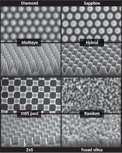
Over the years, we have demonstrated these performance benefits in a great number of common optical materials. Figure 1 shows scanning electron microscope (SEM) images of ARMs textures fabricated in the important laser materials diamond, sapphire, fused silica, and zinc sulfide (ZnS). The figure shows four types of AR textures referred to as motheye, hybrid, subwavelength structure (SWS), and random.
Motheye, hybrid, and random textures are analog variants of graded-index surfaces, and the SWS texture is a binary index variant notable for its ability to achieve extremely low losses at laser wavelengths in any optical material, particularly those for which the optimal refractive index for a thin-film AR coating material does not exist.
Motheye, hybrid, and SWS textures have features that are distributed in a regular array over the optic surface. Such periodic arrays are fabricated through a lithography step to define the pattern in a sacrificial material layer, followed by an etch step to transfer the pattern into the surface of the optic. More recently, TelAztec has developed a process for fabricating a randomly distributed array of features using a single dry-plasma-etch cycle, eliminating the costs associated with lithography.
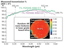
Random-AR (RAR) nanotextures etched in fused silica are readily scaled to large areas, as illustrated by the 20-cm-dia. high-energy laser (HEL) exit aperture prototype shown in Fig. 2. The specific ARM's texture type is determined by the application requirements. Note that for moldable optics, such as many types of glass and chalcogenide materials, a single ARMs-textured master tool can be fabricated in diamond or silicon-carbide templates that are then used to economically replicate the ARMs texture into the surfaces of aspheric lens optics or fiber-optic facets.RAR nanotextures for high-energy pulsed laser optics
For UV laser-system optics, thin-film coatings are particularly sensitive to environmental contamination and are prone to material breakdown due to laser absorption. Recently, RAR textures etched in fused silica have shown great potential for maximizing laser-environment reliability within the multiple-beam high-power laser being developed for fusion-energy production at LLNL.
Random AR textures designed for maximum transmission at the UV laser wavelength of 351 nm were integrated with prototype fused-silica beam-sampling diffraction gratings. The superposition of the RAR and grating-surface structures yielded the desired ~3.5% increase in transmission uniformly over the full aperture, while stabilizing the critical diagnostic grating function. A scanning laser (wavelength of 375 nm) transmission map of a 20-cm-dia. fused-silica window with RAR nanotextures etched in both surfaces is shown as an inset in Fig. 2. A high level of uniformity was achieved with an average transmission of 99.5% calculated for the area within the 17.5 cm circle shown on the map.
RAR textures in fused silica are also notable for wide bandwidth performance, often measuring less than 0.2% loss from 350 through 1064 nm, and less than 0.03% loss for targeted wavelengths from 200 to 1600 nm. Recently, Newport (Santa Clara, CA) made the spectral transmission scans of double-side treated RAR fused silica laser optics shown in Fig. 2. Transmission at the important laser lines of 355 and 532 nm was recorded at 99.7% and 99.8%, respectively. For qualifying any AR treatment, measurements in transmission are much more discriminating than reflection since losses due to scattering and absorption are included in the measurement. The Newport and LLNL data removes any concern regarding potential scatter loss from surface-relief nanotextures.
Of particular interest to LLNL, RAR-textured fused-silica surfaces show a dramatic resistance to adsorption of environmental hydrocarbons compared to sol-gel colloidal silica AR coatings. RAR-treated windows subjected to standardized capillary condensation tests by LLNL were found to adsorb 200 to 400 times less hydrocarbon contaminants compared to NIF baseline-hardened sol-gel AR-coated windows. In addition, the laser transmission of the RAR-treated windows remained unchanged after all exposure levels, whereas the sol-gel-AR coated windows exhibited losses from 1% up to 4.9% after one day of exposure.
This rapid transmission loss due to contaminant adsorption by thin-film coatings for NIF optics, and for many commercial laser-system optics as well, is a longstanding concern. Sol-gel AR coatings are particularly delicate but are used at NIF due to their low cost of application and their high resistance to laser damage-thresholds routinely measured at three to five times that of conventional thin-film AR coatings.
To compare the power-handling ability of the RAR treatment to sol-gel AR coatings, pulsed laser-induced damage testing was conducted by LLNL using its standardized (and unique) large-beam test bed. The laser-damage resistance of the RAR texture was found to be equivalent to the current sol-gel AR coating baseline for NIF fused-silica optics. To relate this result to published commercial thin-film-coating damage testing, a series of RAR-textured fused-silica optics were subjected to ISO standard S-on-1 355 nm, 10 ns pulsed-laser-damage testing at Quantel USA (Bozeman, MT). An average RAR-damage threshold of 26 J/cm2 was found, two times higher than the best performing ion-beam-sputtered thin-film AR coatings reported in the literature and six times higher than catalog high-power laser-window coating specifications.
ARMs for chromium-ion-diffused ZnSe laser-gain media
A serious problem limiting the performance and lifetime of coated optics operating in the mid-IR spectral region (2 to 5 μm) is water absorption. Power scaling of mid-IR tunable laser-gain media based on chromium- or iron-doped ZnSe has been stalled due to water absorption in coatings at wavelengths beyond 2.7μm—the tuning band for Cr2+:ZnSe and the pump-laser band for Fe2+:ZnSe.
Working with the Air Force Research Laboratory (AFRL, Sensors Directorate, Wright Patterson AFB, OH), motheye-type ARMs textures were designed and fabricated in prototype Cr2+:ZnSe laser crystals intended for use in an AFRL test bed. The spectral transmission of the motheye-textured crystals is shown in Fig. 2 compared with identically prepared crystals coated with commercially available thin-film AR material layers. Note that the water-absorption-band losses centered near 2.8 μm for the coated crystals prevent any lasing function, whereas the motheye-textured crystal maintains transmission and can be tuned well beyond 3.1 μm.
With no dissimilar material layers, no water-absorption issues, and the potential to mitigate polishing damage, the etching of motheye AR textures in laser crystals can dramatically increase the power handling capacity of mid-IR lasers. Standardized pulsed-laser-induced damage testing at a wavelength of 2.09 μm was conducted on multiple ARMs-treated ZnSe and Cr2+:ZnSe laser windows by Spica Technologies (Hollis, NH); damage thresholds for the ARMs-treated windows were found to be five times higher than the levels reported for thin-film AR coatings. Recent pulsed laser damage tests conducted by Quantel at a wavelength of 2.94 μm also show damage thresholds for motheye ARMS textures etched in ZnSe that are five times higher than thin-film AR-coated ZnSe.
IPG Photonics (Birmingham, AL) conducted continuous-wave (CW) laser-damage testing at a wavelength of 1.94 μm of ARMs-treated Cr2+:ZnSe windows, measuring a threshold of nearly 0.5 MW/cm2, a level estimated to be at least 50% higher than that of thin-film AR-coated Cr2+:ZnSe gain media. This integrated ARMs approach is now being applied to iron (Fe) doped ZnSe to extend the tunable laser spectral range out to 5.0 μm.
ARMs in sapphire windows for alkali-laser vapor cells
Diode-pumped alkali laser (DPAL) technology is a viable approach to reaching megawatt output power levels, combining the high-conversion efficiency of alkali vapor with inexpensive, compact, electrically driven, diode-laser pump sources. A current barrier to power scaling of DPAL systems is the lack of thin-film AR-coating material options needed to withstand the chemical damage and carbon fouling of the gas-cell windows forming the laser-gain media. Combined with high pump and signal laser power, the alkali-vapor attack rapidly leads to catastrophic surface damage.
An innovative solution to this problem is to etch AR nanotextures in sapphire, a durable material that is not damaged by exposure to alkali vapor. The ARMs texture provides the reduction in losses needed for laser function and a potential resistance to the hydrocarbon adsorption found to foul conventional coated windows in some DPAL configurations (see Fig. 4).
An ongoing Small Business Innovation Research (SBIR) Phase II program sponsored by the U.S. Missile Defense Agency is driving development of ARMs in sapphire for DPAL systems. To date, reflection loss for ARMs-treated sapphire windows below 0.06% has been demonstrated at all relevant DPAL wavelengths in the range of 750 to 950 nm. In alkali-vapor exposure tests conducted by the AFRL, ARMs-treated sapphire windows showed no degradation of the nanostructured surfaces after a six-day trial operating at expected DPAL temperatures and pressures. High-power CW laser-damage testing is scheduled for mid-2014.
RAR-treated fused-silica end facets for fiber lasers
A fiber laser is a silica-based fiber with its core doped with rare-earth elements to function as the active gain medium, with pump light supplied by multiple laser diodes or other fiber lasers. Advantages of fiber lasers include high output power, excellent beam quality, and system reliability. However, the high laser fluence at the fiber entrance and exit facets often requires splicing on a beam-expanding end cap to reduce power density and avoid damage and/or angle-polishing the end facet (adding cost and reducing far-field wavefront quality) to lessen retroreflections back through the fiber. The use of thin-film AR coatings for the highest-power fiber-laser applications is problematic due to power-handling limitations caused by coating absorption and defects, deposition constraints and consistency, and reliability issues.
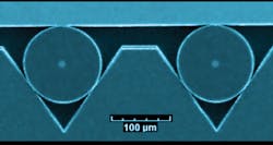
In contrast, the RAR-texture process is readily adapted for fiber-laser facets and end caps.7 Advantages of the RAR approach for fiber-laser facets include a consistent fabrication process, a single material solution for long-term reliability, and high-AR function for low back-reflection with the potential for eliminating angle polishing. RAR textures in fused silica have been measured with losses below 0.03% (−37 dB) at wavelengths of 780, 940, 1064, 1310, and 1550 nm. Figure 5 shows two single-mode fibers mounted in a silicon V-groove block as one example of the many types of fixtures that are compatible with RAR fabrication.In multiple standardized third-party pulsed-laser damage tests comparing RAR textures in fused silica to thin-film AR coatings on fused silica, RAR-treated surfaces have exhibited damage thresholds many times the value found for coatings. In one set of tests conducted by the Army Research Labs (White Sands, NM), RAR-textured fused silica dye-cell laser windows exhibited a damage threshold five times higher than catalog thin-film AR-coated windows specifically designed and sold for high-power laser operation.8
Along with commercially available ARMs textures in materials such as fused silica, BK7, Cr:ZnSe, and sapphire, the ARMs fabrication process is being adapted and performance characteristics quantified in laser materials such as zinc germanium phosphide (tunable mid-IR lasers), diamond (CO2 lasers), YAG, gallium arsenide (diode lasers), and spinel (exit-aperture windows). Microstructure-based wavelength and/or polarization selective reflectors under development are expected to yield similar optical and environmental advantages over existing thin-film coating designs.
REFERENCES
1. S. J. Wilson and M. C. Hutley, "The optical properties of 'moth eye' antireflection surfaces," OpticaActa, 29 (1982).
2. W. H. Lowdermilk and D. Milam, Appl. Phys. Lett., 36, 11, 891 (1980).
3. D. S. Hobbs et al., "Contamination resistant antireflection nanotextures in fused silica for laser optics," Proc. SPIE, 8885, 88850J (2013).
4. K. Schepler and P. Berry, "A promising mid-infrared transition metal laser ion," SPIE Newsroom, http://spie.org/x14261.xml (2007).
5. D. S. Hobbs et al., "Laser damage resistant anti-reflection microstructures for mid-infrared metal-ion doped ZnSe gain media," Proc. SPIE, 8530, 85300P (2012).
6. D. S. Hobbs, "Robust micro-structures in lieu of coatings for AR, HR and filtering in high energy laser systems," High Energy Laser Joint Technology Office Annual Review (May 2013).
7. L. Busse et al., "Anti-reflective surface structures (ARSS) on optics for HELs," High Energy Laser Joint Technology Office Annual Review, (May 2013).
8. D. S. Hobbs et al., "Continued advancement of laser damage resistant optically functional microstructures," Proc. SPIE, 8530, 85300O (2012).
9. A. Bennett et al., "CVD diamond IR optics enable EUV lithography," Laser Focus World, 49, 11, 43–46 (2013).

