IR Imaging: Thin silicon Fresnel lens enables inexpensive thermal-IR imaging
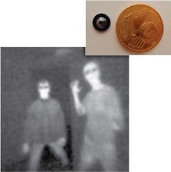
A group of French researchers has designed and fabricated a type of small, thin silicon (Si) Fresnel lens that can simplify compact thermal infrared (IR) cameras and make them lower in cost.1 Although the lens’ resolution is not superb, it is good enough to reveal the presence of a person and some general features. Potential applications for the imager include more affordable surveillance, particularly for home use, the researchers say.
The aspherical lens has a thickness of 1 mm, an f/# of 1.5, and a diameter of just under 4 mm, with the Fresnel surface on the inner (image-facing) side (see figure). The lens stop is placed a bit less than 1 mm in front of the lens at approximately the telecentric position, with the result that edge-of-field rays with a 65° incidence angle are focused by a region of the lens near its edge that hardly overlaps with the lens region focusing the rays with 0° incidence angle. (And of course the chief rays are all parallel to the optical axis due to telecentricity.)
The thinness of the lens allows the use of Si as a refractive optical material in IR spectral regions where it is normally avoided. Importantly, the lens is achromatic over a spectral range of 7 to 14 μm, with the Fresnel surface largely compensating for the dispersion of Si over that range.
The authors say their thin lens design could be a breakthrough in lowering the cost of thermal IR camera lenses by using materials that are cheaper than traditional ones such as germanium and chalcogenide. The researchers are based at ONERA and Institut d’Optique, CNRS (Palaiseau, France) and ULIS (Veurey-Voroize, France).
Superzone diffractive optical element
Fresnel lenses conventionally come in two forms: 1) a “lighthouse” form, which has relatively large individual zones and is only concerned with focusing via refraction (this version has relatively small dispersion due only to the refractive material); and 2) a diffractive version (usually called a “Fresnel zone plate”), which has zones small enough to focus via precisely, stepping the phase of light to produce diffractive focusing (this version has a much larger dispersion due to the spectral nature of diffraction itself).
The new Si lens is an intermediate between the lighthouse and diffractive Fresnel-lens styles.
As Ian Wallhead, staff scientist at Hyperion Development (Lexington, MA), and Alan Kathman of FLIR Optical Components Group (Charlotte, NC) pointed out in a recent LinkedIn discussion (thank you to both), this type of lens is actually well known and called a superzone diffractive optical element (DOE) or multiorder DOE. These lenses have diffractive features that are blazed for higher diffraction orders, rather than the first order, giving lens designers an extra degree of freedom in design.2
The French researchers increased the depth of their lens’ concentric rings and decreased their number to create a multiorder DOE, which reduced the diffractive lens’ chromatic effects to a tolerable level. In tests of the image quality of their prototype, the team found that the image brightness and sharpness uniformity was good enough for a 130° ultrawide-field-of-view imager. They demonstrated that their camera can provide usable images of people inside an office, for example, after commonly used digital post-processing corrections for nonuniformity and distortion were applied to the image.
For imaging, the Si lens was combined with a 160 × 120 pixel bolometer having a 25 μm pixel pitch (the image in this prototype filled only about 80 × 60 pixels, though); the associated electronic module was controlled via a USB interface.
The lens design has been patented, but further work remains to make it marketable at a truly affordable price, says lead author Tatiana Grulois, a Ph.D. candidate at ONERA. The Si lens, with its 50 μm deep features, was fabricated using direct diamond turning; by finding cheaper ways to manufacture the lenses (for example, using photolithography or molding of the appropriate materials), Grulois says her team hopes to reduce the cost of fabricating the optics and drive down the price of the whole imager.
REFERENCES
1. T. Grulois et al., Opt. Lett., 39, p. 3169 (June 2014).
2. Dean Faklis and G. Michael Morris, Appl. Opt., 34, p. 2462 (May 1996).

John Wallace | Senior Technical Editor (1998-2022)
John Wallace was with Laser Focus World for nearly 25 years, retiring in late June 2022. He obtained a bachelor's degree in mechanical engineering and physics at Rutgers University and a master's in optical engineering at the University of Rochester. Before becoming an editor, John worked as an engineer at RCA, Exxon, Eastman Kodak, and GCA Corporation.
