Nonlinear Optics: Nonlinear thin-film mirror frequency-doubles low-power light
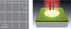
Researchers from the University of Texas at Austin (UT Austin) and the Technische Universität München (Germany) have taken two important, often-used optical components and, via a multi-quantum-well (MQW) semiconductor heterostructure and plasmonic metasurface that is only 450 nm thick, melded them into one. The metasurface (a metamaterial thin enough to be considered 2D) and its underlying heterostructure combine to form a device that is both a mirror and a nonlinear-optical second-harmonic-generation (SHG) element.1
The mirror’s metasurface has a nonlinear optical response a million times stronger than ordinary nonlinear optical materials; the result is a normal-incidence mirror that frequency-doubles light even at relatively low powers. The prototype was designed to frequency-double light at an 8 μm wavelength to 4 μm.
No phase-matching required
In addition (and this is quite important), because the frequency conversion happens over subwavelength scales, the nonlinear mirror does not require matching the phase velocities of the input and output waves; this eliminates a good portion of the design, setup, and tweaking processes that complicate the use of conventional bulk nonlinear crystals.
The new structure can be tailored to work at various frequencies from the near-infrared to the terahertz region and can be designed to produce a giant nonlinear response for other nonlinear optical processes besides frequency-doubling, including sum- and difference-frequency generation, phase conjugation, and a variety of four-wave mixing processes.
About 100 alternating thin-film layers made of indium gallium arsenide (InGaAs) and aluminum indium arsenide (AlInAs), respectively, each between 1 and 12 nm thick, form the heart of the mirror; at the bottom of the structure is a layer of gold. The surface of the mirror is patterned with asymmetrical crossed gold nanostructures (see figure) to form the plasmonic metasurface; this metamaterial structure was designed and fabricated at UT Austin.
Measurements of the SHG light were taken using a focused tunable 30-mW-emitting quantum-cascade laser supplying the fundamental frequency; the intensity at the mirror was on the order of a few kilowatts per square centimeter. The conversion efficiency of the first prototype device was between 0.1% and 0.2%.
The material’s giant nonlinear effect (greater than 5 × 10⁴ pm/V) arises from the coupling of electromagnetic modes in the metasurface with electronic intersubband transitions in the carefully tailored semiconductor thin-film stack. To test the robustness of the design, the researchers intentionally fabricated some metasurfaces with slightly changed design parameters and still measured a similarly large nonlinear response (large detunings produced little or no nonlinear response, also as expected).
Other semiconductors possible
The researchers used InGaAs and AlInAs in their device, but other semiconductors, such as those based on InGaAlN, AlGaAs, or indium gallium arsenide antimonide (InGaAsSb), could lead to differing characteristics.
“GaN-based materials can enable the creation of similar structures in the near-infrared and visible spectral ranges,” says Mikhail Belkin, assistant professor of electrical and computer engineering at UT Austin. “GaN/AlGaN/InGaN heterostructures may have extremely large conduction band offsets (>2 eV) that allow, in principle, engineering electron subbands with energy spacings that correspond to near-IR and visible frequencies. However, currently, the interface quality of GaN/AlGaN/InGaN heterostructures is significantly worse than that for InGaAs/AlInAs/InP. Poor interface quality between semiconductor layers leads to transition linewidth broadening and reduction of attainable optical nonlinearities.”
Belkin notes that another option is to use GaAs/AlGaAs heterostructures, which have a very high interface quality. “However, GaAs/AlGaAs has a slightly smaller conduction band offset (and also larger effective mass, which negatively affects transition dipole-moment values) compared to InGaAs/AlInAs,” he notes. “Therefore, we chose the latter for our experiment. Other heterostructures, such as the InGaAsSb family, may be used to push the operation of our structures to near-infrared. If using different semiconductors, metal nanoresonator dimensions would have to be changed, but this is relatively straightforward.”
The researchers list many types of nonlinear optical structures and effects that can potentially be created. For example, voltage-tunable and active electrically pumped nonlinear metasurfaces are two interesting possible structures; frequency downconversion, mixing, phase conjugation, all-optical control and tunability, and photon-pair generation are some nonlinear optical processes that may someday be achieved using these metasurfaces.
REFERENCE
1. Jongwon Lee et al., Nature (2014); doi:10.1038/nature13455.

John Wallace | Senior Technical Editor (1998-2022)
John Wallace was with Laser Focus World for nearly 25 years, retiring in late June 2022. He obtained a bachelor's degree in mechanical engineering and physics at Rutgers University and a master's in optical engineering at the University of Rochester. Before becoming an editor, John worked as an engineer at RCA, Exxon, Eastman Kodak, and GCA Corporation.
