Raman Spectrometers: Low-cost Raman spectrometer uses concave grating and CMOS SPAD
An essential component of a Raman spectrometer is the wavelength-selector element (filter or monochromator) that is used to separate the incident light spatially according to the wavelength. By focusing on miniaturization and suppression of fluorescence using a concave grating and a complementary metal-oxide semiconductor (CMOS)-based time-gated single-photon avalanche diode (TG-SPAD) detector, researchers at McMaster University (Hamilton, ON, Canada) have developed a low-cost Raman spectrometer targeted at portable inline water-monitoring applications.1
Miniaturization via a concave grating
Monochromator-based spectrometers typically use planar gratings and multiple mirrors/lenses for wavelength separation. A concave grating performs both light separation and focusing, reducing optical path lengths and miniaturizing the system footprint. However, miniaturization must be traded off against resolution. Using a holographic technique, the grating was fabricated using an ultraviolet laser on a plano-concave lens with a 38.6 mm radius of curvature to form a grating with a 980 nm grating constant. The surface was sputter-coated with 2.5 nm of chromium and 20 nm of gold to make it reflective.
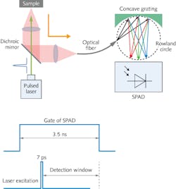
In the experimental setup, light from a 532 nm solid-state laser source (to be replaced by a cheaper laser diode in a final low-cost configuration) passes through a dichroic mirror and is focused on the sample. The target reflected signal is then collected and focused into an optical fiber, the other end of which is positioned on the virtual Rowland circle formed by the radius of curvature of the concave grating (see figure). For this setup, the shorter-wavelength components (anti-Stokes Raman and Rayleigh) are transmitted through the dichroic mirror, while the longer-wavelength components (Stokes scattering and fluorescence) are reflected and coupled into the fiber and to the grating.
Cost reduction via a CMOS SPAD
For Raman measurements, a single time-gated SPAD pixel is mounted on a three-axis translation stage and scanned in coarse (10 μm) and fine (1 μm) increments over a 4 mm range to acquire spectral data from 520 to 600 nm—the spectral window that corresponds to the Raman shifts of most chemical and biological samples from 500 cm-1 to 2000 cm-1.
The time-gated SPAD detector is turned on in a very narrow gate window, detecting only those photons coincident with that window. Three on-chip pulse generators are used to achieve fast gating of the SPAD for speeds from 3 ns to 250 ps. Analysis of the spectrum of Rhodamine B under different detection windows reveals that the 3 ns window sees a high fluorescence peak that is easily suppressed by using a narrower detection window. By subtracting the background fluorescence from the full signal spectrum, the Raman peaks are easily distinguished for Rhodamine B.
After fitting the Raman peak data with Gaussian curves, average values of Rhodamine B spectra of 1372 cm-1 and 1284 cm-1 are in good agreement with the 1365 cm-1 and 1290 cm-1 values obtained by more expensive (and physically larger) surface-enhanced Raman spectrometer (SERS) instruments. For full-width half-maximum (FWHM) measurements of Raman peaks, the entrance slit width of this low-cost Raman setup is determined by the 200 μm multimode fiber diameter of the fiber used to couple light into the Rowland circle of the grating (compared to 10–25 μm entrance slits for more expensive, higher-resolution spectrometers). This fiber diameter, however, can certainly be modified to improve FWHM measurements.
This low-cost, portable setup is made possible by the 0.13 μm CMOS SPAD and the customized concave grating. Although a single-pixel detector was used to test the design, a pixel array will be designed for the final integrated system to simplify the measurement and reduce the data-acquisition time.
The CMOS SPAD achieves a temporal resolution of 60 ps. If combined with a time-to-digital converter (TDC), this temporal resolution is beneficial to extract the timing information of the signal, such as the photon-emission time according to the excitation; currently, a pixel array with integrated TDC is being designed. This integrated system could not only provide the Raman spectra data like commercial Raman spectrometers do, but could also track the photon-emission times.
"Such a micro-Raman spectrometer would be a very powerful, low-cost, compact, portable inline water-monitoring system targeting chemical and microbiological contaminants," says McMaster University professor M. Jamal Deen. "The micro-spectrometer could also be used to identify other molecules in micro-sized samples for a variety of applications such as drug discovery or materials research through the sample's 'Raman fingerprints.'"
REFERENCE
1 Zhiyun Li and M. Jamal Deen, Opt. Express, 22, 18736–18747 (July 28, 2014).
About the Author

Gail Overton
Senior Editor (2004-2020)
Gail has more than 30 years of engineering, marketing, product management, and editorial experience in the photonics and optical communications industry. Before joining the staff at Laser Focus World in 2004, she held many product management and product marketing roles in the fiber-optics industry, most notably at Hughes (El Segundo, CA), GTE Labs (Waltham, MA), Corning (Corning, NY), Photon Kinetics (Beaverton, OR), and Newport Corporation (Irvine, CA). During her marketing career, Gail published articles in WDM Solutions and Sensors magazine and traveled internationally to conduct product and sales training. Gail received her BS degree in physics, with an emphasis in optics, from San Diego State University in San Diego, CA in May 1986.
