Photonic Frontiers: Nitride VCSELS: Nitride VCSELs pose a tough challenge

Gallium nitride has been a huge success in blue edge-emitting diode lasers, so developing it for vertical-cavity surface-emitting lasers (VCSELs) seems a logical step. VCSELs have important advantages for some applications, including lower thresholds, better beam quality, easy production of dense two-dimensional arrays, higher-speed direct modulation, and wafer-level testing. Gallium-arsenide (GaAs) VCSELs are highly successful, and in the laboratory nitride VCSELs advanced in a few years from optical pumping to electrical pumping at room temperature. A new blue light source seemed in the offing.
But lately nitride VCSEL progress has slowed. They "still exhibit severe performance limitations" largely arising from the nature of nitride compounds, Joachim Piprek of NUSOD Institute (Newark, DE) wrote last year in an assessment of the field.1 Peak powers remain below a milliwatt. Only a handful of top labs have demonstrated nitride VCSELs, and those successes have come only with cutting-edge research techniques that are far from mass production.
The VCSEL challenge
First proposed in the 1970s, VCSELs took time to develop because of their complex fabrication requirements. Very highly reflective mirrors are needed to extract power efficiently from an optical cavity perpendicular to the thin active layer of a diode laser. The standard approach in GaAs is epitaxial deposition of many alternating thin layers of two GaAs alloys to form a distributed Bragg reflector (DBR). Ideally, the rear cavity mirror should be 99.9% reflective, with the output mirror somewhere in the range of 99.7% reflective, says Daniel Feezell of the University of New Mexico (Albuquerque).
Those are tough specifications, but they are possible with GaAs, which Piprek calls "the perfect material" for VCSELs. A key advantage is small variation of lattice spacing with GaAs composition, allowing lattice matching of alloys with high-index contrast during epitaxial deposition. However, no suitable pairs of lattice-matched alloys with high refractive index are available in either gallium nitride (GaN) or indium phosphide (InP), making fabrication of very high-reflectivity DBRs far more challenging than in GaAs. All-dielectric DBRs are an alternative, but they pose other problems described later.
A related problem is that dielectric DBRs are not conductive, requiring intra-cavity contacts, and the conductivity of p-GaN is too low for it to be used to deliver current evenly to the active region. Developers can add a layer of indium tin oxide (ITO), a semi-transparent conductor, but ITO has its own limits. "Its conductivity is insufficient to evenly distribute current for device apertures greater than about 10 micrometers," Feezell wrote in a recent review.2 Moreover, its optical loss is significant at ultraviolet and visible wavelengths, so its placement in the cavity is critical.
A further complication comes from the short length of the cavity, only a few micrometers. It's crucial to align the cavity's standing-wave profile so the peaks are aligned in the quantum wells in the active layer, and any lossy layers, such as the ITO, are at nulls. Moreover, peak gain in the quantum well must match a resonant wavelength in the cavity.
Making GaN VCSELs
The first to meet the challenge of electrically pumping a GaN VCSEL were Tien-Chang Lu and colleagues at the National Chiao Tung University (Hsinchu, Taiwan) in 2008, although operation was limited to liquid nitrogen temperature. They took a hybrid mirror approach, with one semiconductor DBR and one dielectric DBR, as shown in Figure 1. Starting on a sapphire substrate, they first epitaxially grew a DBR from 29 pairs of AlN and GaN layers, then n-type GaN, and an active layer containing multiple InGaN/GaN quantum wells. On top, the researchers deposited 240 nm of ITO to spread current across a 10 µm aperture, then added a dielectric DBR with alternating layers of Ta2O5 and SiO2. Achieving 99.4% reflectivity and avoiding cracks in their epitaxial nitride DBR were major factors behind their success in reporting laser operation with a 1.4 mA threshold, but they did not report the maximum power.3
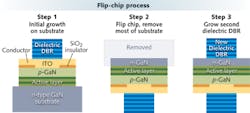
Later that year, Yu Higuchi and colleagues at Nichia (Tokushima, Japan) demonstrated room-temperature operation with a pair of dielectric DBRs. This avoided the need to fabricate a crack-free nitride DBR, but required a complex flip-chip process (see box on "Flip-chip VCSEL fabrication" on p. 33). They first grew the active layer on a sapphire substrate, then added p-type GaN, a 50 nm IT layer, and an Nb2O5/SiO2 DBR, then bonded the DBR layer to a conductive silicon substrate. Next, they removed the sapphire substrate from the wafer and deposited a second dielectric DBR on that surface, as shown in Figure 2. That helped them report room-temperature continuous-wave output of 0.14 mW at 414.4 nm and a drive current of 12 mA.More improvements followed. Nichia researchers switched to GaN substrates, reducing defect levels and increasing CW output to 0.62 mW. They also increased operating lifetime, but noted that threshold current increased after only 10 minutes.4 The National Chiao Tung group reached room-temperature with a series of refinements including improving current flow and contacts and reducing ITO thickness to 30 nm to reduce optical loss.5
More entries and new approaches
The pace seemed to step up in 2012 with three more groups posting noteworthy results.
Panasonic (Kyoto, Japan) reported CW room-temperature operation at up to 3 µW with dual-dielectric DBRs made from alternating layers of ZrO2 and SiO2. They reported VCSELs with both short 2 µm cavities for quasi-singlemode oscillation and long 6 µm cavities for multimode operation, and reported a 5-by-5 planar array, a first for nitride VCSELs. Panasonic said at the time that multimode emission was attractive for arrays because they would reduce speckle in applications such as laser displays or energy-efficient solid-state lighting.6 In an invited update presented in early 2014, Masao Kawaguchi of Panasonic cited technical challenges including series resistance of ITO and p-GaN and charge separation in polar GaN quantum wells.7
Looking toward easing manufacture, Nicolas Grandjean's group at the Swiss Federal Polytechnic Institute (EPSL) (Lausanne) in 2012 reported fabricating hybrid monolithic VCSELs with epitaxial DBRs containing Al0.18In0.82N layers lattice-matched to GaN. They grew defect nitride DBRs on a c-plane GaN substrate, then deposited an active layer containing five quantum wells, an electron blocking layer, and a top TiO2/SiO2 dielectric DBR. They did not reach CW operation, but reported pulses over 300 µW. They claimed their approach would ease processing and increase yield and chip quality.8
A team at the University of California at Santa Barbara (UCSB) headed by Feezell before he moved to New Mexico was the first to grow GaN VCSELs on a nonpolar substrate, the m-plane of GaN. "The main advantages of nonpolar material are that the gain is higher and the polarization is pinned along a known direction of the crystal, important for the many polarization-sensitive applications," he says. They used dual-dielectric DBRs in the structure shown in Figure 3 to get high reflectivity, but developed a photo-electrochemical removal process so one expensive substrate could yield many VCSELs. That flip-chip removal process also produces uniform cavity thickness, important in aligning standing waves with quantum wells for maximum power. In 2012, the researchers reported peak power of 19.5 µW at 412 nm.9 A follow-on paper in July 2014 verified cavity length control and reported VCSELs made from the same wafer were polarized in the same direction.10Other refinements continue. In June 2014, Wen-Jie Liu and colleagues at Xiamen University (Xiamen, China) announced a dual-dielectric DBR VCSEL with linewidth of only 0.12 nm, corresponding to a Q value of 3570, but output power was only 0.5 µW.11 The following month, Piprek described a computer simulation that placed a tunnel diode in the active layer, which could double the output power by distributing carriers more uniformly among the quantum wells.12
Outlook
"All the groups have done a great job just getting these things to work," says Feezell. He blames the current slowdown largely on a lack of funding, but notes that projects at Panasonic and Nichia show companies the potential for long-term profit.
Both the lifetime and output power of today's nitride VCSELs are too low, says Ehsan Hashemi of Chalmers University (Goteborg, Sweden). "The prospects of nitride VCSELs are quite bright," he adds, but we need "better technological solutions to overcome the material constraints."
"Some of the biggest roadblocks we have faced are obtaining highly conductive, smooth, and transparent ITO using methods that avoid plasma damage to p-type GaN," says John Leonard, who recently took over UCSB's nitride VCSEL project. He wants ITO films with <1 nm RMS smoothness to reduce scattering losses. "We may need completely different materials than ITO," says Feezell. He says other big issues are DBRs, spreading drive current across the aperture, polarization control, and cavity length control.
"It will take both money and some revolutionary ideas" to make high-performance nitride VCSELs a reality, says Feezell. "Ultimately, we will have nitride VCSELs, but it will take more time to get there."
References
1. J. Piprek, "What is the problem with GaN-based VCSELs?" at NUSOD 2013 Conference, http://www.nusod.org/2013/nusod13_WB1.pdf.
2. D. Feezell, "The evolving GaN VCSEL," Compd. Semicond. (March 2014), http://www.compoundsemiconductor.net/article/91717-the-evolving-gan-vcsel.html.
3. T. C. Lu et al., "CW lasing of current injection blue GaN-based vertical cavity surface emitting laser," Appl. Phys. Lett. 92, 141102 (2008); doi:10.1063/1.2908034.
4. K. Omae et al., Appl. Phys. Express 2, 052101 (2009), http://iopscience.iop.org/1882-0786/2/5/052101.
5. T. C. Lu et al., Appl. Phys. Lett. 97, 071114 (2010), http://scitation.aip.org/content/aip/journal/apl/97/7/10.1063/1.3483133.
6. T. Onishi et al., IEEE J. Quant. Electron. 48, 1107 (2012); doi:10.1109/JQE.2012.2203586.
7. M. Kawaguchi et al., Proc. SPIE 8986, 89861K, (2014); doi:10.1117/12.2037484.
8. G. Cosendey, et al., Appl. Phys. Lett. 101, 151113 (2012); doi:10.1063/1.4757873.
9. C. Holder et al., Appl. Phys.Express 5, 092104 (2012); doi:10.1143/APEX.5.092104.
10. C. O. Holder et al., Appl. Phys. Lett. 105, 031111 (2014), doi:10.1063/1.4890864.
11. W.-J. Liu et al., Appl. Phys. Lett. 104, 251116 (2014); doi:10.1063/1.4885384.
12. J. Piprek, Appl. Phys. Lett. 105, 011116 (2014); doi:10.1063/1.4887377.
Flip-chip VCSEL fabrication
Nitrides generally cannot be grown on a dielectric DBR layer so fabrication of a dual-dielectric DBR VCSEL requires processing beyond the usual epitaxial growth on a substrate. First, the active layer, p-type layer, contact layer, and one dielectric layer are grown on a substrate, typically GaN. Next, the chip is turned over and most of the substrate is removed by etching or a less destructive process. Finally, the second dielectric DBR layer is grown on what had been the chip's bottom so both top and bottom of the VCSEL are highly reflective.

Jeff Hecht | Contributing Editor
Jeff Hecht is a regular contributing editor to Laser Focus World and has been covering the laser industry for 35 years. A prolific book author, Jeff's published works include “Understanding Fiber Optics,” “Understanding Lasers,” “The Laser Guidebook,” and “Beam Weapons: The Next Arms Race.” He also has written books on the histories of lasers and fiber optics, including “City of Light: The Story of Fiber Optics,” and “Beam: The Race to Make the Laser.” Find out more at jeffhecht.com.
![FIGURE 2. Flip-chip fabrication produced the first CW room-temperature nitride VCSEL at Nichia. Structures from the n-GaN down were fabricated on a sapphire substrate, then the chip was flipped, the sapphire etched away, and the second DBR fabricated on top [4]. FIGURE 2. Flip-chip fabrication produced the first CW room-temperature nitride VCSEL at Nichia. Structures from the n-GaN down were fabricated on a sapphire substrate, then the chip was flipped, the sapphire etched away, and the second DBR fabricated on top [4].](https://img.laserfocusworld.com/files/base/ebm/lfw/image/2016/01/1410lfw01f2.png?auto=format,compress&fit=max&q=45&w=250&width=250)

