Technology Review: Top 20 technologies for 2014 cover the range from basic R&D to new apps
This past year's round of innovation in photonics encompasses everything from basic and applied R&D to new applications and technical improvements.
Display glasses you'd want to wear
1. Augmented-reality displays.
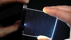
To the larger world, one of the most prominent forms of photonics gear in development is the eyeglasses-style head-worn display. The Google Glass, however, has not had much success in its introduction. Why? Well, it's strange-looking; it has only a single, small screen off to the side; and the user often appears cross-eyed while using it (the potential intrusiveness of a video-taking pair of glasses is yet another problem, of course). Researchers at the University of North Carolina at Chapel Hill (UNC) and Nvidia Research (Durham, NC) now have an eyeglasses-display design that could eliminate all these problems: augmented-reality glasses that are transparent, can be stereo for 3D, and at least have the potential to look like a pair of eyeglasses (see Fig. 1 and see "Augmented-reality displays: Pinlight arrays enable lightweight, see-through head-worn display," Laser Focus World (LFW), Oct. 2014, World News; http://bit.ly/1xMIoa7).
2. The "perfectly bad" optical surface.
As for much higher performance optical systems, such as telescopes or high-energy laser optics, what can be done when a precisely designed and fabricated optical system, after assembly, still has unwanted wavefront error? Or, conversely, what might an optical systems designer do to reduce the cost, complexity, and alignment sensitivity of such a system without losing its low wavefront error?
The engineers at QED Optics (Rochester, NY) have an answer: armed with a magnetorheological finishing (MRF) machine, they can fabricate an optical plate that has the precise inverse wavefront error and thus cancels out the wavefront problems when placed at the right spot in the optical system (see "Test and Measurement: MRF fabricates 'perfectly bad' surfaces," LFW, Feb. 2014; http://bit.ly/1ubGktg).
3. Superlenses for microscopy.
Just as augmented-reality glasses seem to the tech consumer a revolutionary idea that has not yet surmounted the large hurdles preventing it from wide use, so do metamaterial superlenses seem to the photonics specialist. Well, those hurdles are still there, but progress is being made in superlenses intended for subwavelength microscopy (a "superlens" captures and refocuses not only far-field light, but also evanescent waves, thus beating the traditional diffraction limit). For example, a 1D multilayer metamaterial lens developed at the University of California at San Diego (La Jolla) takes a near-field object and images it in the far field, changing the evanescent waves to free-space propagating waves. Another superlens created at Purdue University (West Lafayette, IN) can be machined into the end of an optical fiber. A third approach to fabrication, self-assembly, is being studied at the University of Southampton (England) (see "Photonic Frontiers: Microscopy: New twists on superlenses improve subwavelength microscopy," LFW, Aug. 2014; http://bit.ly/1xxuXfT).
4. Negative-index layers in thin-film coatings.
In the area of multilayer optical thin-film coating design, Michel Lequime and collaborators at the Fresnel Institute (Marseille, France) have taken a look at what can be done when certain layers in a thin-film design are made to have a negative refractive index. (Prototypes of such materials are already being developed in the form of metamaterials.) The group has determined through numerical calculations that negative-index layers can help tailor the spectral dispersion of a quarter-wavelength Bragg mirror and, more interestingly, achieve very wideband resonant behavior for a multilayer Fabry-Perot cavity. This type of cavity, consisting of two multilayer reflectors sandwiching a thin-film center, is a standard approach to designing multilayer optical filters (see "Negative-index layers in multilayer optical coatings lead to novel properties," LFW, May 2014, Newsbreaks; http://bit.ly/1zjKSxM).
5. Exawatt-class laser glass.
Research into laser glass materials for exawatt-class lasers is underway. Because laser output at exawatt-power levels will likely be achieved by simultaneously shortening the duration of the laser output pulse while keeping the laser aperture large to prevent damage from high laser fluence, Ti:sapphire crystals are out of the running, as they can't be made to the meter-class apertures required. Scientists at Schott North America (Duryea, PA) are developing neodymium (Nd)-doped phosphate and other types of doped glass that can handle the intense pulses of light of an exawatt laser. Such lasers may use one type of glass for the front-end optical parametric chirped-pulse amplifier (OPCPA) and other types (Nd:silicate and Nd:phosphate) for the final amplification stage (see "Laser Glass Materials: Glass advances usher in exawatt-class lasers," LFW, April 2014, World News; http://bit.ly/10ZjHwt).
Spectral conquests
6. Visible tunable fiber lasers.
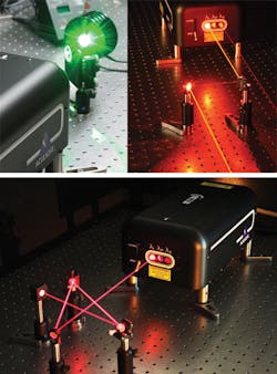
Fiber lasers overcome many of the limitations of traditional lasers: they are often smaller (fewer bulky optics), simpler (fiber-optic pigtailed pump lasers), and higher in wall-plug efficiency. But, gain materials suitable for use in fiber lasers emit in only a few limited wavelength ranges, mostly in the near-IR. However, they can be used to pump other lasers or optical parametric oscillators (OPOs) that reach into and tune across regions within the visible spectrum. While some of the fiber laser's innate simplicity is lessened, the resulting device is still compact and efficient. Versions created at Lockheed Martin Laser and Sensor Systems (Bothell, WA) include frequency-doubled erbium and ytterbium fiber lasers producing tunable red, and doubled Raman fiber lasers tuning between red and green (see Fig. 2). Research is ongoing to reach through the rest of the visible spectrum (see "Advances in Light Sources: Fiber lasers tune to the visible," LFW, June 2014; http://bit.ly/1xhsgkh).7. Blue-emitting VCSELs.
Vertical-cavity surface-emitting lasers (VCSELs) serve many purposes, from data communications to night-vision illumination, but so far the emission wavelengths of production VCSELs have remained in the red spectral region or in the IR. However, efforts are continuing to develop nitride-based VCSELs that emit in the blue. Why is this research being highlighted here if there has not yet been any commercial success, and indeed many hurdles remain? It's here simply because the blue VCSEL, which could be one of those game-changing photonics devices, has been created in the lab, and projects at Nichia (Anan, Japan), Panasonic (Osaka, Japan) and elsewhere where there is enough funding continue undaunted. "It will take both money and some revolutionary ideas" to make high-performance nitride VCSELs a reality, says Daniel Feezell of the University of New Mexico (Albuquerque). "Ultimately, we will have nitride VCSELs, but it will take more time to get there." Keep at it, folks! (See "Nitride VCSELs pose a tough challenge," LFW, Oct. 2014; http://bit.ly/1GP3pHg.)
8. Concentric-grating terahertz QCLs.
An international team of researchers from Nanyang Technological University (NTU) and the Singapore Institute of Manufacturing Technology (both in Singapore), as well as the University of Leeds (England), Hong Kong Polytechnic University (Kowloon), and Shanghai Jiao Tong University (China), has shown that, at least for terahertz-emitting quantum-cascade lasers (QCLs), geometry can make a big difference. Rather than creating a standard ridge-waveguide QCL, they designed and fabricated a device with a circular active region and a concentric circular grating (CCG) that couples the output perpendicularly into free space. The advantage: a low-divergence tens-of-milliwatts output that is five times more powerful than that of ridge-waveguide terahertz QCLs (see "Terahertz Sources: Concentric-grating terahertz QCLs five times more powerful than ridge QCLs," LFW, Feb. 2014; http://bit.ly/1pR5GwI).
9. Perovskite VCSELs.
And then there's perovskite, the versatile photonic material (actually, class of materials) that is being made into light emitters as well as high-efficiency thin-film photovoltaic solar cells. Researchers at the University of Cambridge's Cavendish Laboratory (England) have created optically pumped perovskite VCSELs that convert green pump light to near-IR (760 nm) laser light with a 70% efficiency. One of the findings from this demonstration is that upon light absorption, electrons and holes are formed very quickly in the perovskite (within 1 ps), but then take anywhere up to a few microseconds to recombine. These properties actually bode well for the most widely researched area for perovskite—the development of low-cost, efficient solar cells (see "High-efficiency perovskite photovoltaic material also lases," LFW online, March 28; http://bit.ly/1pR96zu).
10. Perovskite high-brightness LEDs.
In another example, a hybrid perovskite can be formed into high-brightness LEDs that emit green, red, or near-IR light. They are fabricated extremely simply by spin-coating a perovskite solution onto a substrate. "The big surprise to the semiconductor community is to find that such simple process methods still produce very clean semiconductor properties, without the need for the complex purification procedures required for traditional semiconductors such as silicon," says professor Sir Richard Friend of the Cavendish Laboratory. The increasing quantum efficiencies of the LEDs at higher current densities could enable low-cost LEDs for lighting and displays (see LFW online, Aug. 5; http://bit.ly/1zjO7Fo).
Vortex charges for higher data rates
11. Orbital-angular-momentum multiplexing.
Conventionally, fiber-optic data rates are increased through approaches that combine light from separate emitters, such as wavelength-division multiplexing (WDM; combining many different wavelengths) or polarization-division multiplexing (PDM; combining different polarizations). Now, another version can be thrown into the mix: orbital-angular-momentum (OAM) multiplexing. In OAM, laser beams of differing helical phases (also called "vortex charges") are combined for transmission over optical fiber, then demultiplexed at the receiving end. The research, done at the University of Southern California (USC; Los Angeles), the Jet Propulsion Lab (JPL; Pasadena, CA), the University of Glasgow (Scotland), and Tel Aviv University (Israel), led to transmission rates of 100 Tbit/s, relying on PDM and WDM as well as OAM (see "Free-Space Communications: 100 Tbit/s link uses orbital-angular-momentum multiplexing," LFW, March 2014, World News; http://bit.ly/1v3pkYd).
12. Diamond multiwavelength light source.
It may not be too long before a diamond becomes a communication engineer's best friend: a team from Harvard University, Massachusetts Institute of Technology (MIT), and the Schlumberger-Doll Research Center (all in Cambridge, MA) has been looking at the nonlinear optical properties of diamond in a ring-resonator configuration. The team has demonstrated a prototype single-crystal diamond multiwavelength ring-resonator telecom light source that works as an optical parametric oscillator (OPO) via four-wave mixing. The result when pumped by a continuous-wave laser is a frequency comb. The researcher are also positing the production of frequency combs in the visible spectrum for precision astronomy (see Nonlinear Materials: Diamond nonlinear-wave-mixing promises multiwavelength telecom source," LFW, Sept. 2014, World News; http://bit.ly/1EtR33n).
13. Fiber-optic explosives sensor.
Sensitive detection of explosives is becoming ever-more important; gas- or fluid-based fiber-optic sensing, with its potential for long light/chemical interaction regions, is a logical approach. Scientists from the University of Adelaide (Australia), the Defence Science & Technology Organisation (DTSO; Edinburgh, Australia), and the Shanghai University of Electric Power (China) have created a suspended-core microstructured optical fiber, deposited a conjugated-polymer coating on its inside surface and used simple capillary action to fill it with acetone tainted with small amounts of the explosive 1,4-dinitrobenzene (DNB). When carrying light with 488 nm wavelength, the fiber exhibits fluorescence quenching of the surface-attached polymer when the explosive is present, even at concentrations down to 6.3 ppm. The technique could be further developed for detection of homemade improvised explosive devices (see "Coated suspended-core fiber detects trace explosives," LFW, June 2014, World News; http://bit.ly/1umMaI8).
14. Machinable F-P cavities for fiber sensing.
In a technique invented by Yi Liu and Shiliang Qu of the Harbin Institute of Technology (Weihai, China), high-quality Fabry-Perot interferometer (FPI) cavity sensors can be carved into single-mode silica optical fiber using femtosecond-laser-induced water-breakdown machining. The resulting FPI cavity, suitable for measuring the refractive index of fluids, is only 40 μm long and has flat axial surfaces. Pulses from a Ti:sapphire laser were focused onto the fiber, which was immersed in water to machine the silica via bubble, shock wave, and high-speed jet creation. The sensor has low sensitivity to temperature and can measure refractive index to an accuracy of 1.29 x 10⁻⁴ refractive-index units (see "Femtosecond laser carves refractive-index-sensing F-P cavity in optical fiber," LFW, Jan. 2014, Newsbreaks; http://bit.ly/14dqXXv).
SWIFTS miniature spectrometer
15. Spectral detection using nanodot lineups.
The stationary-wave integrated Fourier-transform spectrometer (SWIFTS), a new spectroscopic instrument being developed by Resolution Spectra Systems (Meylan, France), does not face the traditional problems associated with grating and Fourier-transform spectrometers, which are trade-offs between resolution, measured wavelength range, speed, size, and long-term calibration stability. The detection portion of SWIFTs consists of nanodots periodically positioned in a waveguide; scattered light from each nanodot is picked up by a different pixel in a linear-array detector (see Fig. 3). As a result, due to the different standing waves produced in the waveguide, the spectrum at each nanodot is different; a mathematical transform called a Lippman function is applied to the data to produce the overall spectrum. Being waveguide-based, the spectrometer is small and rugged. It is suitable for characterizing spectra of laser sources such as VCSELs, OPOs, external-cavity laser diodes, and others, as well as interrogating many fiber-Bragg-grating sensors at once in a remote fiber-optic sensor cable (see "Spectroscopy: High-resolution spectrometers shrink down with SWIFTS," LFW, Sept. 2014; http://bit.ly/11hQYUn).16. Single-photon lidar.
A lidar system that is sensitive to single photons and can map low-reflectance tree canopies as well as high-reflectance ice and snow surfaces from a nominal air-to-ground altitude of 2.3 km has been developed by engineers at Sigma Space Corp. (Lanham, MD); the system is an improvement over an older one that sampled at lower rates. In Sigma's recently commercially introduced, self-funded, moderate-altitude high-resolution quantum lidar system, which is humbly called HRQLS (pronounced Hercules), a green laser beam is spatially split to form a 5 × 5 array that produces 50 cm ground pixels at a height of 2.3 km (see Fig. 4). For the nominal 2.3 km flying height, maximum half-cone angle of 20°, and maximum airspeed of 450 km/hr, the maximum areal coverage is 616 km2/hr, almost eight times that of the earlier system. Also built by Sigma was a custom 100-beam single-photon lidar that can operate at a 8.5 km air-to-ground height with a swath width of 2.4 km (see "Single-photon lidar yields rapid topographic and bathymetric coverage," LFW, July 2014, World News; http://bit.ly/1qDXDOC).
17. High-fill-factor silicon photomultipliers.
Silicon photomultipliers (SiPMs) have been developed as possible alternatives to traditional photomultiplier tubes (PMTs), but the polysilicon (poly-Si) electrical resistors of the device must sit on the detector's surface, blocking part of the incoming light. To improve the photon-detection efficiency of SiPM devices, researchers at A*STAR Institute of Microelectronics (Singapore) have developed a new technique where vertical bulk-Si quenching resistors are embedded into SiPM cells to replace the conventional poly-Si resistors. Results from both simulations and experiments confirm the performance of the new SiPM cell structure; a SiPM with a cell fill factor of 81% has been fabricated (see "Single-photon Counting: New silicon photomultiplier structure promises more efficient photon detection," LFW, May 2014; http://bit.ly/1sDRlz2).
18. Quantum-dot LCDs.
The liquid-crystal display (LCD) is indispensable to the average person's life (at least in so-called developed countries; they are fast becoming more used in developing countries, too); the absence of LCDs would bring many an engineer, accountant, Wikipedia intellectual, and compulsive-texting tweener to a mental standstill.
So any improvement on the standard LCD is more than welcome; engineers at 3M have complied by developing and bringing to market the first LCDs that contain quantum dots (QDs). These displays can cover a color gamut up to 50% larger than that covered by conventional LED-lit LCDs and can even exceed that of commercial organic LED (OLED) displays. The QDs are dispersed in a polymer matrix sandwiched between water-impermeable barrier films, forming a sheet just 55 μm thick. Current-generation QDs have a lifetime to 30,000 h, while the next generation is expected to have at least a 70,000 h lifetime (see "Advances in Displays: Quantum dot film lets LCDs express 50% more color," LFW, April 2014; http://bit.ly/1v3ras0).
19. White-light diffraction tomography.
A new tomography technique developed at the University of Illinois (Champaign) produces 3D image renderings of cells and their internal structure using conventional microscopes and white-light sources. The technique promises to acquire such 3D images without the disadvantages of using chemicals, ultraviolet radiation, or mechanical forces—approaches used in other 3D-imaging microscopy techniques. The resulting images capture what the cell is doing under normal circumstances, rather than under chemical (dye or contrast agent) duress (see Fig. 5). The white-light diffraction tomography (WDT) device mounts to a conventional phase-contrast microscope with no modification to the microscope itself. The microscope shifts its focus through the depth of the cell, capturing images of various focus planes. Software then compiles the images into a coherent 3D rendering. Because the cells are not damaged in any way, videos of cells are easily taken (see LFW online, Jan. 22; http://bit.ly/1EBNGcG).
20. Starbug motion control.
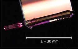
Scientists at the Australian Astronomical Observatory, which is developing next-generation ground telescopes that require many hundreds of fiber-optics to be independently positioned at a telescope's focus (each fiber picks up the light from a different star), faced the problem of how to position all these fibers so that they could be independently moved across the large glass surface at the focus. Rather than inventing a massive, unbuildable mechanical mess, the scientists invented Starbugs, which are small, piezoelectrically driven cylindrical robots that, held by vacuum, can each march to their own tune at speeds as fast as 2 mm/s or in steps as small as 1 μm.
Starbugs have just three main parts: a piezoceramic tube, held within another piezoceramic tube by a solid ring at one end. They are low in cost and, if needed, can operate in crowds of thousands at once (see Fig. 6 and LFW, March 2014; http://bit.ly/1xMTwDW).

John Wallace | Senior Technical Editor (1998-2022)
John Wallace was with Laser Focus World for nearly 25 years, retiring in late June 2022. He obtained a bachelor's degree in mechanical engineering and physics at Rutgers University and a master's in optical engineering at the University of Rochester. Before becoming an editor, John worked as an engineer at RCA, Exxon, Eastman Kodak, and GCA Corporation.


