VCSELS for Manufacturing: High-power VCSEL arrays make ideal industrial heating systems
ARMAND PRUIJMBOOM
Many industrial manufacturing processes use some kind of thermal process for melting, drying, curing, annealing, or diffusing. The types of heaters used range from hot-air blowers, gas burners, and convection ovens to halogen lamps, induction heaters, and microwave ovens. All these approaches have their specific merits, but for a significant fraction of industrial heating needs, vertical-cavity surface-emitting laser (VCSEL)-based photonic heating has advantages.
VCSELs have a brightness 100 to 1000 times higher than that of halogen lamps and can be switched on and off in milliseconds. Furthermore, they allow accurate dosing control for either very homogeneous heating of large areas or the imposition of heat patterns with local variations in the deposited energy density. In addition, solid-state light sources like VCSELs are very robust and have lifetimes exceeding multiple 10k hours of continuous operation.
VCSEL arrays are distinctly different from the world of conventional high-power laser diodes. The latter is dominated by lasers for cutting or welding steel, where it is all about what laser system has the highest brightness and power to cut even faster through even thicker steel. VCSELs are more benign lasers that can also be scaled to very high power by massive parallel operation of millions of microlasers. Because of this multibeam concept, their effective brightness is lower, and while they are not suited for metal machining, they are an excellent solution for industrial heating.1
VCSEL geometry
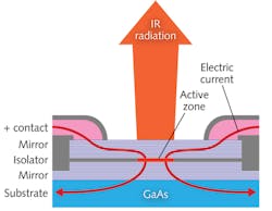
The cavity of a VCSEL is formed perpendicularly to the surface of a gallium arsenide (GaAs) wafer by epitaxial growth of layers with alternating refractive index, forming so-called distributed Bragg reflectors (DBRs), called "DBR mirrors" (see Fig. 1). Usually, n-type doped DBR mirrors are formed first, followed by quantum wells forming the active layer and p-type doped DBR mirrors forming the emission facet. The current flows through a ring-shaped contact on the upper mirrors to the substrate.
A current confinement aperture, usually formed by selective oxidation of an aluminum-rich layer in the middle of the cavity, is introduced to improve the optical-electrical conversion efficiency by only electrically pumping the area that overlaps with the optical modes. The emission wavelength can range between about 800 and 1100 nm, depending on the design of the quantum well and the cavity.
Depending on the aperture size, which can range between 4 and 20 μm, one VCSEL can emit 1 to 10 mW of power. The VCSEL cavities (often referred to as "mesas" because of their shape) have a diameter of 30 to 40 μm; when hexagonally arranged, more than 500 of them can be placed on one square millimeter of a chip, leading to power densities of several watts per square millimeter.
An advantage VCSELs have over edge-emitting laser diodes is that the laser arrays are fully completed by wafer processing; functional testing and chip selection can be done by wafer probing. The chip assembly can be done with standard automatic semiconductor processes and equipment for pick-and-place and wire-bonding. As a result, costs are comparable to those for LEDs.
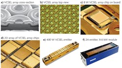
Philips Photonics has scaled VCSEL technology to allow fabrication of very large arrays. For example, an array chip of 1.9 × 2.0 mm2, containing more than 2000 VCSELs, is assembled on a board to form an illumination module for night-vision cameras (see Figs. 2a-c). Depending on the heat-sink temperature, it emits more than 8 W of infrared power. A larger 2D array can then be formed by assembling the same chips next to each other (see Fig. 2d). By series connection of the chips, the current stays low (the same as that for a single chip) and the voltage high, allowing cost-effective driver design.Figure 2e shows a 400 W emitter, including the cooling structure. The emitting area is 8.5 × 40 mm2 and consists of 56 chips arranged in four rows of 14 chips, two of which are connected in series to form emitting zones of 4.2 × 40 mm2. Each zone can be independently adjusted between 0 and 200 W output power.
Scalable by stacking
These VCSEL modules are easily scalable: Larger arrays can be created by stacking these emitters next to each other. Figure 2f shows a 9.6 kW module with an emitting area of 40 × 200 mm2. The power density, which is above 1 W/mm2, can be enhanced to above 10 W/mm2 by higher output-power densities of the VCSEL chip and further by the use of microlenses and secondary optics.2,3 The performance characteristics of an 808 nm emitter show that an output power above 400 W is achieved at 40% power-conversion efficiency. An even higher power is possible at lower efficiency.
High performance of densely packed large-area arrays is much more challenging to achieve than for a single chip assembled on a heat sink. In the latter case, lateral heat spreading leads to 3D heat conduction, whereas for a densely packed emitter the heat conduction is essentially one-dimensional. Despite this challenging thermal situation, performance of the large-area arrays is on par with benchmark results.
An electronic driver unit has been developed that can drive up to 12 zones of a maximum of six emitters. The response time is 5 ms, allowing fast switching of the laser power between 0 and 100% of its maximum power. An EtherCAT industrial bus interface enables software control of the power. The calibration data of an emitter is stored on an SD memory card, which allows the user to set the true output power. Safety switches are included which, for example, switch off the power when the cooling water is interrupted.
Together with the scalable modules shown in Figure 2f, the electronic driver forms a "heating system" that allows control of the heating dose spatially as well as temporally. At a 30 mm distance from the emitter surface, the mixing of radiation from the individual chips evens out the gaps between the chips, leading to a ripple in the received optical intensity of less than 5%.
Local control of heating
With these heating systems, large areas can be heated homogeneously. The system's zoning allows for alteration of the power locally to adjust for conditions such as locally higher heat conduction at the edges of a workpiece. Between 800 and 1100 nm, the wavelength can be chosen for maximum absorption of the material. A major advantage compared to halogen lamps is that, when dimming the output, the wavelength—and hence the material absorption-does not change.
In conveyor-belt ovens, the entire oven needs to be heated up to heat materials within it, which requires a long time and hence long ovens for high throughput. In contrast, VCSEL-based photonic heating systems are much more compact due to their much higher power density, as well as the fact that the infrared (IR) radiation only has to heat the workpiece rather than the entire oven. The fast switching allows the system to switch off when there are gaps between the materials on the belt.
Heat patterns can be generated on linearly moving materials by switching the output power spatially as well as temporally. This can be used for belt-oven-like processes such as sintering of screen-printed thick films for passive electronic components and solar cell manufacturing. This approach can also be used in roll-to-roll processes, which have been recently pursued for cheap and efficient manufacturing of printed electronics, organic LEDs (OLEDs), and solar cells.
VCSEL heating systems are compact and easy to integrate as compared to other approaches. To date, VCSEL arrays are successfully used for melting and welding of plastics, as well as fast firing for solar-cell manufacturing. Tape laying of carbon-fiber-reinforced thermoplastic composites, which is a special case of plastic welding, is used for weight savings in the aerospace industry, and more recently also in the automotive industry.
In the automotive industry, high-strength steel is used to save weight. Local softening of this steel facilitates cold-forming of automotive parts. It has been demonstrated that VCSELs enable treating larger areas without the use of scanning systems.4 On a 1.5-mm-thick steel sample, an 8.5 × 40 mm2 large area was heated to 900°C by a VCSEL module. The Vickers hardness was measured at different locations as a function of the distance from the area that remained cold (see Fig. 5). A more than 50% reduction in Vickers hardness is observed in the treated area. Material analysis confirms that the initial martensitic structure observed in the untreated area is converted to the softer ferrite and cementite structure in the heated area.
Currently, traditional laser diodes or even fiber and disk lasers are used in conjunction with complicated, bulky, and expensive optics to generate a homogeneous illumination for heating. In contrast, VCSEL illumination systems are a compact, efficient, and cost-effective solution for demanding heat-treatment applications requiring outstanding homogeneity.
REFERENCES
1. H. Moench and G. Derra, "High power VCSEL systems," Laser Technol. J., Wiley, no. 2 (2014).
2. H. Moench et al., "Modular VCSEL solution for uniform line illumination in the kW range," Proc. SPIE 8241, 824110 (2012).
3. H. Moench et al., "VCSEL arrays with integrated optics," Proc. SPIE 8639, 86390M (2013).
4. S. Wollgarten, Fraunhofer ILT, unpublished.
Armand Pruijmboom is general manager of Philips GmbH, Photonics Aachen (Aachen, Germany), a branch of Philips Photonics; e-mail: [email protected]; www.philips.com/photonics.

