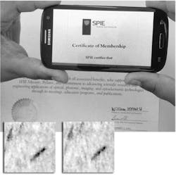
Optical microstructures act as secure product identifiers
Researchers at the University of Geneva (Carouge, Switzerland) have developed a set of algorithms to robustly ascertain an object’s authenticity using optically acquired microstructures. These microstructures have intrinsically random surface properties that cannot be cloned and thus serve as a unique identifier. The basic application envisions that packages or objects, such as watches or passports (or an SPIE certificate) are photographed on the factory line with an industrial camera. To authenticate an object, a second image can be taken in the field with a consumer mobile phone after which the software compares both images.
Two sets of algorithms have been developed. The first extracts an image patch from a predefined region and compensates any geometrical or lighting distortions prior to quantization and matching. This is done by comparing a printed mark, such as part of a corporate logo, to a stored template. Two distinct advantages of compensating geometric distortions in this fashion is the fact that this allows the deployment of traditional decorrelation and fingerprinting techniques so that only the hash values need to be stored. Furthermore, the microstructures may be modeled as Gaussian noise realizations. The second algorithm uses adapted computer-vision features to validate a potential match. It can find relatively robust features in the visually poor microstructures and its matching procedure can handle data sets that contain more than 50% outliers. The university has also produced the first publicly available database of forensic authentication microstructure optical sets (FAMOS) for testing and benchmarking at http://sip.unige.ch. Reference: S. Voloshynovskiy et al., SPIE Newsroom (Dec. 1, 2014); doi:10.1117/2.1201411.005524.
