Nanophotonics: Cubic nanoantennas (nanocubes) efficiently direct light
Researchers at Monash University (Clayton, Victoria, Australia) have developed cube-shaped, tiny, resonant optical antennas that improve over spherical nanoantennas for directing ultranarrow beams of light where needed for potential applications in food safety, pollutant identification, and disease diagnosis.1 These cubic dielectric nanoparticles, or “nanocubes,” operate with minimal optical loss and heating and offer high packing densities and relative ease of fabrication.
Unidirectional light scattering
Generally, the scattering of light from a subwavelength nanoantenna occurs symmetrically in both forward and backward directions using either magnetic or electrical resonance properties. For nanoantennas simultaneously possessing both types of resonances, unidirectional forward scattering patterns are obtained via scattering cancellation in the backward direction by destructive interference between the electric and magnetic responses. Different plasmonic nanostructures demonstrate such directional scattering properties, but unfortunately are often high in loss and produce heat, which limits their scattering applications in the visible and infrared (IR) regions.
Therefore, for visible and near-IR operation, lossless dielectric nanoantennas are a logical choice. However, in most cases the intensity of directional scattering from the conventional semiconductor nanoparticle antennas is fairly weak, as directionality is obtained far away from the scattering resonance. Metallic core/dielectric shell nanoparticles can achieve unidirectionality around the resonance frequency, thus enhancing directional scattering intensity; but again, high loss and heating in the core limit their practical use.
To combat these drawbacks, the Monash University researchers have developed lossless nanocube antennas (composed of insulating, rather than conducting or semiconducting materials) that achieve directional resonant scattering through interference of spectrally overlapping electric and magnetic modes in the visible and near-IR region. The unidirectional forward scattering profiles are azimuthally symmetric, providing highly tunable beam width and intensity, with minimal backscattering for light-focusing applications.
Dielectric nanocube chains
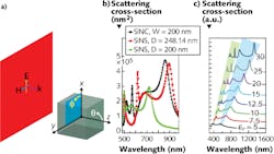
For a cubic silicon nanoparticle, stronger scattering of a plane wave can be observed as compared to an equivolume or equidimensional spherical silicon nanoparticle (see figure). Much larger scattering intensity and better directionality are obtained for dielectric nanocubes with relative permittivity much lower than silicon. While scattering capability also depends on the permittivity value of the nanocube, unidirectional scattering can be further optimized and tailored by using a linear chain of identical nanocubes.
By placing nanocubes operating in a unidirectional mode adjacent to each other, there exists an optimal interparticle gap that can result in minimized side lobes and more efficient light propagation in one direction with engineered beam width and intensity. This gap can be determined as a function of operating wavelength, particle size, and permittivity value. By adjusting the number of nanocubes in the chain and the gap between them, one can finely tune the features of the focused beam.
“These ultranarrow directional beams can play multiple roles in lab-on-a-chip devices such as illumination sources in microfluidic analysis or minute deflection registers in nanocantilever-based sensors or as ‘optical nanoscanners’ for targeting specific molecules,” says Debabrata Sikdar, Monash University’s Victoria India Doctoral Scholar in the department of Electrical and Computer Systems Engineering. “Their nanofocusing capability even has applications in futuristic high-density 5D optical data storage, where data can be manipulated by selectively focusing light into a small portion of the memory elements, or these nanocubes can serve as ‘optical vias’ providing interlayer connectivity between 3D-integrated multicore ICs of the future, replacing the lossy interconnects to ensure ultrafast loss-less computing.”
REFERENCE
1. D. Sikdar et al., J. Appl. Phys. 117, 083101 (2015); http://dx.doi.org/10.1063/1.4907536.

Gail Overton | Senior Editor (2004-2020)
Gail has more than 30 years of engineering, marketing, product management, and editorial experience in the photonics and optical communications industry. Before joining the staff at Laser Focus World in 2004, she held many product management and product marketing roles in the fiber-optics industry, most notably at Hughes (El Segundo, CA), GTE Labs (Waltham, MA), Corning (Corning, NY), Photon Kinetics (Beaverton, OR), and Newport Corporation (Irvine, CA). During her marketing career, Gail published articles in WDM Solutions and Sensors magazine and traveled internationally to conduct product and sales training. Gail received her BS degree in physics, with an emphasis in optics, from San Diego State University in San Diego, CA in May 1986.
