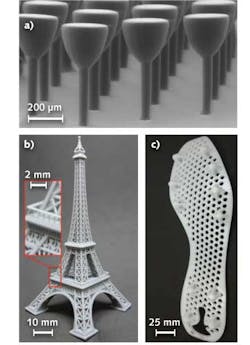
Using a continuous liquid interface production (CLIP) polymerization process, Carbon3D (Redwood City, CA), which is working with researchers at the University of North Carolina (Chapel Hill, NC) and North Carolina State University (Raleigh, NC), can fabricate 3D-printed objects tens of centimeters in size with 100 μm resolution in minutes (500 mm/hour rates possible), as opposed to the hours required for stepwise layer-by-layer photopolymerization methods used in conventional 3D printing.
Unlike traditional bottom-up stereolithography printers whereby ultraviolet (UV) light exposure, resin renewal, and part movement are conducted in separate, discrete steps, the CLIP process projects a continuous sequence of images in UV light generated through a digital light-processing unit onto an oxygen-permeable, UV-transparent window below a liquid resin bath. An oxygen-containing dead zone inhibits photopolymerization above the window and maintains a liquid interface below the advancing part. As the curing part is drawn out of the resin, suction forces constantly renew reactive liquid resin that cures to form the object. This dead zone is maintained by adjusting the photon flux rate of the source, the concentration of photoinitiator in the resin, and the resin curing dosage, determined by the reactivity of the resin. Carbon3D is able to apply the entire polymer chemistry textbook and make parts that range from hard prototyping and engineering resins to elastomers, completely biodegradable materials, and materials that would be useful for casting of metal. Reference: J. R. Tumbleston et al., Science, 1349–1352 (Mar. 20, 2015); http://dx.doi.org/10.1126/science.aaa2397.

Gail Overton | Senior Editor (2004-2020)
Gail has more than 30 years of engineering, marketing, product management, and editorial experience in the photonics and optical communications industry. Before joining the staff at Laser Focus World in 2004, she held many product management and product marketing roles in the fiber-optics industry, most notably at Hughes (El Segundo, CA), GTE Labs (Waltham, MA), Corning (Corning, NY), Photon Kinetics (Beaverton, OR), and Newport Corporation (Irvine, CA). During her marketing career, Gail published articles in WDM Solutions and Sensors magazine and traveled internationally to conduct product and sales training. Gail received her BS degree in physics, with an emphasis in optics, from San Diego State University in San Diego, CA in May 1986.