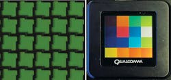
Thin-film MEMS pixels create color-rich ambient-light display
Reflective displays that depend on ambient light in applications that require very low power consumption often suffer from low brightness and/or poor color gamut since the color pixels used typically absorb two-thirds of the incident light. But a new interferometric absorption design from researchers at Qualcomm MEMS Technologies (San Jose, CA) has pixels that can be tuned through a continuum of colors—including high-contrast black and white reflectance states—with high brightness and color-rich performance.
The interferometric configuration consists of individual microelectromechanical system (MEMS)-actuated pixels comprised of a mirror, a thin metallic absorbing (but also transmissive) layer, and an air gap in between. Within each pixel, the incident and reflected light interfere with each other and create standing-wave patterns with a periodicity—adjusted by mirror movement and air-gap changes—that corresponds to a particular wavelength (and color) of light. These individual mirrors have maximum mirror sag of less than 10 nm across their 74 μm pitch and have been assembled into 1.58 in. diagonal arrays with 384 × 384 pixels that demonstrate 40% reflectance and 50% color gamut for a completely diffuse ambient light input with viewing at 8° off surface normal. These capabilities are a significant improvement compared to conventional RGB-pixel-based reflective displays, including the first-generation RGB-based Mirasol display from Qualcomm. Other factors such as specially designed front-of-screen diffusers or lighting conditions that involve a mixture of diffuse and directed light can significantly increase both the reflectance and color gamut numbers. Reference: John Hong et al., Optica, 2, 7, 589–597 (2015).

Gail Overton | Senior Editor (2004-2020)
Gail has more than 30 years of engineering, marketing, product management, and editorial experience in the photonics and optical communications industry. Before joining the staff at Laser Focus World in 2004, she held many product management and product marketing roles in the fiber-optics industry, most notably at Hughes (El Segundo, CA), GTE Labs (Waltham, MA), Corning (Corning, NY), Photon Kinetics (Beaverton, OR), and Newport Corporation (Irvine, CA). During her marketing career, Gail published articles in WDM Solutions and Sensors magazine and traveled internationally to conduct product and sales training. Gail received her BS degree in physics, with an emphasis in optics, from San Diego State University in San Diego, CA in May 1986.
